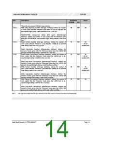
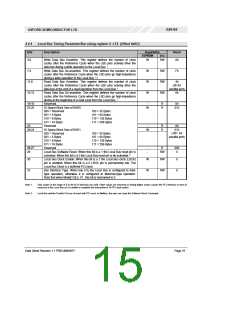
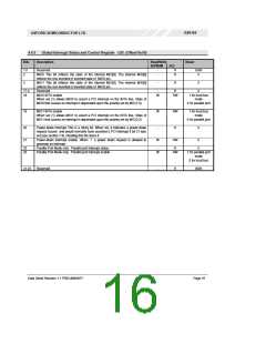
OX9162
OXFORD SEMICONDUCTOR LTD.
4.6 Power Management
the MIO state that asserts the INTA line (if that option were
to be enabled). This means that when the external device
is not interrupting it will begin the powerdown cycle. For
greater flexibility in the generation of the power down
request,, a powerdown filter is also available to ensure that
the relevant MIO pins remain stable for a selectable period
before a powerdown request is issued.
The OX9162 is compliant with PCI Power Management
Specification Revision 1.0. The function implements its own
set of Power Management registers and supports the
power states D0, D2 and D3. Power management is
accomplished by power-down and power-up requests,
asserted via interrupts and the PME# pin respectively. The
PME# pin is de-asserted when the sticky PME_Status bit is
cleared in both functions.
Function0 implements the PCI Power Management power-
states D0, D2 and D3. Whenever the device driver
changes the power-state to state D2 or D3, Function0
takes the following actions:-
Power-down request is not defined by Power Management
1.0. It is a device-specific feature and requires a bespoke
device driver implementation. The device driver can either
implement the power-down itself or use a special interrupt
and power-down features offered by the device to
determine when the device is ready for power-down.
·
The Local Bus clock pin, LBCK, is disabled regardless
of the programmed value in LT2[30].
The PCI interrupt for Function0 is disabled.
Access to I/O or Memory BARs of Function0 is
disabled.
·
·
However, access to the configuration space is still enabled.
The device driver can optionally assert/de-assert any of its
selected (design dependant) MIO pins to switch off VCC,
disable other external clocks, or activate shut-down modes
to any external devices on the Local Bus.
The PME# pin can, in certain cases, activate the PME#
signal when power is removed from the device, which will
cause the PC to wake up from Low-power state D3(cold).
To ensure full cross-compatibility with system board
implementations, use of an isolator FET is recommended.
If Power Management capabilities are not required, the
PME# pin can be treated as no-connect.
Function0 can issue a wake up request by using the MIO
pins. When MIC[7] or MIC[6] is set, rising or falling edge of
the relevant MIO pin will cause Function0 to issue a wake
up request by setting PME_Status = (PMCSR[15]), if it is
enabled by PMCSR[8] of Function0. PME_Status is a
sticky bit which will be cleared by writing a ‘1’ to it. After a
wake up event is signalled, the device driver is expected to
return the function to the D0 power-state.
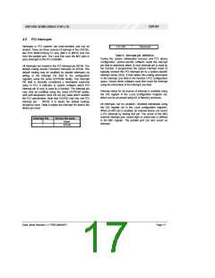
4.6.1 Power Management using MIO
The power-down request for the Local Bus is application-
dependent. Provided that the necessary enables have
been set in the local registers, the multi-purpose I/O pins
MIO(1:0) can be used to generate a powerdown request.
The MIO state that governs powerdown is the inverse of
Data Sheet Revision 1.1 PRELIMINARY
Page 18

 OXFORD [ OXFORD SEMICONDUCTOR ]