OX9162
OXFORD SEMICONDUCTOR LTD.
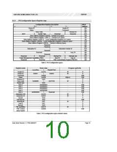
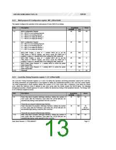
4.4.2 Multi-purpose I/O Configuration register ‘MIC’ (Offset 0x04)
This register configures the operation of the multi-purpose I/O pins ‘MIO[1:0] as follows.
Bits
Description
Read/Write
EEPROM
Reset
PCI
1:0
MIO0 Configuration Register
W
RW
00
00 -> MIO0 is a non-inverting input pin
01 -> MIO0 is an inverting input pin
10 -> MIO0 is an output pin driving ‘0’
11 -> MIO0 is an output pin driving ‘1’
3:2
MIO1 Configuration Register
W
RW
00
00 -> MIO1 is a non-inverting input pin
01 -> MIO1 is an inverting input pin
10 -> MIO1 is an output pin driving ‘0’
11 -> MIO1 is an output pin driving ‘1’
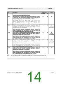
4
5
MIO0_PME Enable. A value of ‘1’ enables MIO0 pin to set the
PME_Status in PMCSR register, and hence assert the PME# pin if
enabled. A value of ‘0’ disables MIO0 from setting the PME_Status bit.
MIO1_PME Enable. A value of ‘1’ enables MIO1 pin to set the
PME_Status in PMCSR register, and hence assert the PME# pin if
enabled. A value of ‘0’ disables MIO1 from setting the PME_Status bit.
MIO0 Power Down Request: A ‘1’ enables MIO0 to control the power
down request filter.
W
W
RW
RW
0
0
6
W
W
-
RW
RW
R
0
0
7
MIO1 Power Down Request: A ‘1’ enables MIO1 to control the power
down request filter.
Reserved
31:8
00
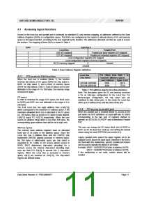
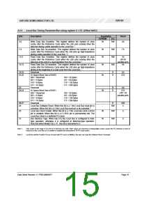
4.4.3 Local Bus Timing Parameter register 1 ‘LT1’ (Offset 0x08):
The Local Bus Timing Parameter registers (LT1 and LT2) define the operation and timing parameters used by the Local Bus.
The timing parameters are programmed in 4-bit registers to define the assertion/de-assertion of the Local Bus control signals.
The value programmed in these registers defines the number of PCI clock cycles after a Reference Cycle when the events
occur, where the reference Cycle is defined as two clock cycles after the master asserts the IRDY# signal. The following
arrangement provides a flexible approach for users to define the desired bus timing of their peripheral devices. The timings refer
to I/O or Memory mapped accesses.
Bits
Description
Read/Write
EEPROM
Reset
PCI
3:0
Read Chip-select Assertion (Intel-type interface). Defines the number of
clock cycles after the Reference Cycle when the LBCS[1:0]# pins are
asserted (low) during a read operation from the Local Bus.1
W
W
W
RW
0h
These bits are unused in Motorola-type interface.
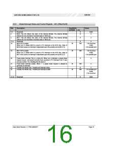
7:4
Read Chip-select De-assertion (Intel-type interface). Defines the number
of clock cycles after the Reference Cycle when the LBCS[1:0]# pins are
de-asserted (high) during a read from the Local Bus. 1
RW
RW
3h
(2h for
parallel port)
These bits are unused in Motorola-type interface.
11:8
Write Chip-select Assertion (Intel-type interface). Defines the number of
clock cycles after the Reference Cycle when the LBCS[1:0]# pins are
asserted (low) during a write operation to the Local Bus. 1
0h
Data Sheet Revision 1.1 PRELIMINARY
Page 13

 OXFORD [ OXFORD SEMICONDUCTOR ]