VS1005g Datasheet
10 VS1005 PERIPHERALS AND REGISTERS
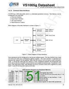
10.10 Common Data Interfaces
Vs1005 has a 3kB data buffer which is a dedicated peripheral memory. The memory can be
configured to be used with:
• Ethernet interface
• Nand Flash Interface
• SD Card Interface
• Reed-Solomon Codecs
Block diagram of the data interfaces is shown in figure 11.
Figure 11: Block Diagram of Data Interfaces.
Each peripheral can be configured to use its own address space. The dsp interface has a read
and write port with auto incrementing address register. The read operation is pipelined and
requires two reads to fill the pipeline. After that the memory can be read on each instruction
cycle. It should be noted that the memory is time multiplexed between the peripherals and
some idle cycles are required if several devices are enabled simultaneously. A guideline is that
every 16th read cycle is idle. Dsp interface has Error Correctin Code (ECC) registers for nand
flash. It uses 2D xor to protect and correct data.
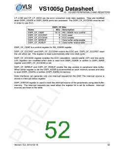
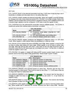
DSP Interface Registers for Peripheral Memory
Reg Type Reset Abbrev
Description
0xFC66
0xFC67
0xFC68
0xFC69
0xFC6A
0xFC6B
0xFC6C
r
r
0
0
0
0
0
0
0
LP_LOW
ECC line parity register bits [15:0]
CP_LP_HIGH ECC column parity bits [5:0] and line parity bits [17:16]
DSPI_CF
DSPI_ADDR
DSPI_ODATA Memory write port for dsp
DSPI_IDATA
DSPI_ST
r/w
r/w
r/w
r
Dsp interface control
Memory address register for dsp interface, 11 bits
Memory read port for dsp
Interrupt status register for data buffer peripherals
r/w
Version: 0.2, 2012-03-16
51

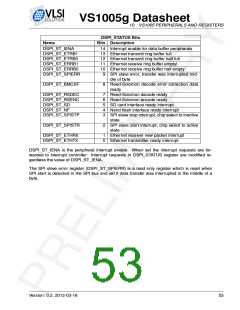
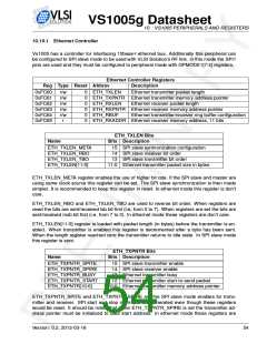
 ETC [ ETC ]