VS1005g Datasheet
10 VS1005 PERIPHERALS AND REGISTERS
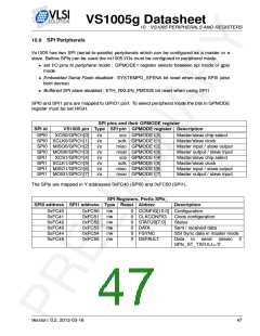
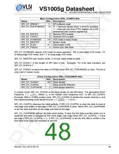
Main Configuration SPIx_CONFIG Bits
Bits Description
Name
SPI_CF_SRESET
11 SPI software reset
SPI_CF_RXFIFOMODE
10 ’0’ = interrupt always when a word is received,
’1’ = Interrupt only when FIFO register full or CS
deasserted with receive register full
SPI_CF_RXFIFO
SPI_CF_TXFIFO
9
8
Receive FIFO enable
Transmit FIFO enable
SPI_CF_XCSMODE
SPI_CF_MASTER
SPI_CF_DLEN
7:6 xCS mode in slave mode
Master mode
4:1 Data length in bits
Frame sync idle state
5
SPI_CF_FSIDLE
0
SPI_CF_XCSMODE selects xCS mode for slave operation. ’00’ is interrupted xCS mode, ’10’
is falling edge xCS mode, and ’11’ is rising edge xCS mode.
SPI_CF_MASTER sets master mode. If not set, slave mode is used.
SPI_CF_DLEN+1 is the length of SPI data in bits. Example: For 8-bit data transfers, set
SPI_CF_DLEN to 7.
SPI_CF_FSIDLE contains the state of FSYNC when SPI_ST_TXRUNNING is clear. This bit is
only valid in master mode.
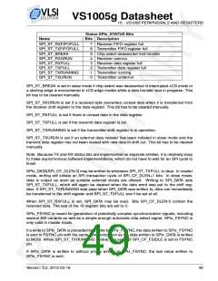
Clock Configuration SPIx_CLKCONFIG Bits
Name
Bits Description
SPI_CC_CLKDIV
SPI_CC_CLKPOL
SPI_CC_CLKPHASE
9:2 Clock divider
1
0
Clock polarity selection
Clock phase selection
In master mode, SPI_CC_CLKDIV is the clock divider for the SPI block. The generated SCLK
fm
frequency f = 2×(c+1) , where fm is the master clock frequency and c is SPI_CC_CLKDIV.
Example: With a 12 MHz master clock, SPI_CC_CLKDIV=3 divides the master clock by 4, and
12MHz
2×(3+1)
the output/sampling clock would thus be f =
= 1.5MHz.
SPI_CC_CLKPOL reverses the clock polarity. If SPI_CC_CLKPOL is clear the data is read at
rise edge and written at fall edge if SPI_CC_CLKPHASE is clear. When SPI_CC_CLKPHASE
is set the data is written at rise edge and read at fall edge.
SPI_CC_CLKPHASE defines the data clock phase. If clear the first data is written when xcs is
asserted and data is sampled at first clock edge (rise edge when SPI_CC_CLKPOL = 0 and
fall edge if SPI_CC_CLKPOL = 1). If SPI_CC_CLKPHASE is set the first data is written a the
first data clock edge and sampled at second.
Version: 0.2, 2012-03-16
48

 ETC [ ETC ]