VS1005g Datasheet
10 VS1005 PERIPHERALS AND REGISTERS
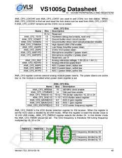
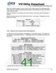
ANA_CF3_2GCNTR register is used to match VCO’s center frequency to programmed value
(CCF). ANA_CF3_DIV[1:0] controls the VCO’s dividers. These dividers are used to set VCO’s
output frequency range.
ANA_CF3_480ENA is the 480 MHz clock driver enable for UTM. When set the clock driver is
enabled.
ANA_CF3_GAIN1 and ANA_CF3_GAIN2 set the ADC 1 and 2 gains. ADC gain can be ad-
justed to four values.
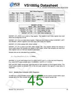
ADC Gain
Register value
Gain
001
010
100
20dB (max)
17dB
14dB
000 11dB (min), default after reset
10.6.2 Regulator and Peripheral Clock Control Registers
Vs1005 has four internal regulators, one regulator for each power domain. The voltage can
be adjusted in about 50mV step size. To save power some of the peripheral clocks can be
switched off.
Regulator and Clock Control
Reg Type Reset Abbrev
Description
0xFECE
0xFED0
r/w
r/w
0
0
REGU_CF
REGU_VOL Regulator voltage register
Regulator control register
REGU_VOL Bits
Name Bits Description
REGU_CF_AVDD[4:0] 14:10 Analog voltage configuration 2.7V-3.6V
REGU_CF_IOVDD[4:0]
REGU_CF_CVDD[4:0]
9:5
4:0
IO voltage configuration, 1.8V-3.6V
Core voltage configuration, 1.65V-1.9V
REGU_CF Bits
Name Bits Description
REGU_CF_SNFVOL1 11:7 Serial Flash voltage configuration
REGU_CF_SNFOFF
REGU_CF_ADOFF
REGU_CF_FMOFF
REGU_CF_REGCK
REGU_CF_AOFF
REGU_CF_IOOFF
REGU_CF_COFF
6
5
4
3
2
1
0
Serial Flash voltage regulator shutdown
AD filter clock gate control
FM demodulator clock gate control
Regulator latch enable
Analog voltage regulator shutdown
IO voltage regulator shutdown
Core voltage regulator shut down
1
User should not modify this register if embedded serial flash is used.
Version: 0.2, 2012-03-16
41

 ETC [ ETC ]