VS1005g Datasheet
10 VS1005 PERIPHERALS AND REGISTERS
10.6 XTAL Clock Domain Registers
Peripheral control registers control the logic that is clocked with xtal clock (12MHz).
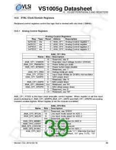
10.6.1 Analog Control Registers
Analog Control Registers
Reg Type Reset Abbrev
Description
0xFECB
0xFECC
0xFED2
0xFED3
r/w
r/w
r/w
r/w
0
0
0
0
ANA_CF1 Analog Control register 1
ANA_CF0 Analog Control register
ANA_CF2 Analog Control register 2
ANA_CF3 Analog Control register 3
ANA_CF1 Bits
Name Bits Description
15 Reserved, use ’0’
ANA_CF1_VHMON 14 Regulator input voltage monitor (VHIGH)
ANA_CF1_PWRBTN 13 Power button pin state
ANA_CF1_BTNDIS 12 Power button reset disable
11 Reserved, use ’1’
ANA_CF1_DBG 10 Debug mode pin state
ANA_CF1_XTDIV
ANA_CF1_SARPD
9
8
7
6
Input clock divider for 24 MHz xtal oscillator
SAR power down
Reserved, Use ’0’
ANA_CF1_DAPD
DAC power down
ANA_CF1_DAGAIN 5:4 Reserved, use ’00’
ANA_CF1_DRVPD
3
2
DAC driver power down
Reserved, use ’0’
1:0 Reserved, use “00”
ANA_CF1_XTDIV is the input clock prescaler control register. When register is set the input
clock is divided by 2. ANA_CF1_SARPD, ANA_CF1_DAPD and ANA_CF1_DRVPD are analog
module’s enable signals. When register is set the module is enabled.
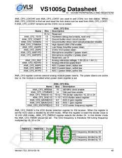
ANA_CF0 Bits
Name Bits Description
15:11 Reserved, use ’00000’
ANA_CF0_M1LIN
ANA_CF0_M2LIN
10
9
8:6
5
4
3
Line input mode select for ADC 1
Line input mode select for ADC 2
Reserved, use ’000’
Mic input mode select for ADC 2
2 GHz vco lock status
ANA_CF0_M2MIC
ANA_CF0_LCKST
ANA_CF0_LCKCHK
ANA_CF0_M1MIC
ANA_CF0_M21
2 GHz vco lock check init
2
1:0
Mic input mode select for ADC 1
ADC 2 and 1 RF mode “11” / Alternate line input
pin select (“00” default, “01” pins 71/70, ‘”10”
pins 68/67)
Version: 0.2, 2012-03-16
39

 ETC [ ETC ]