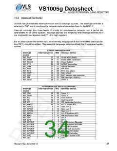
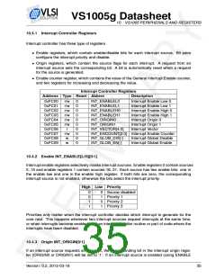
VS1005g Datasheet
10 VS1005 PERIPHERALS AND REGISTERS
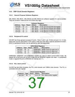
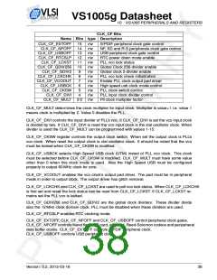
CLK_CF Bits
Name Bits type Description
CLK_CF_EXTOFF 15 r/w
S/PDIF peripheral clock gate control
NF, SD and R-S peripherals clock gate control
USB peripheral clock gate control
RTC power down mode enable
PLL vco lock status
Global Clock 256-divider enable
Global clock 2-divider enable
PLL vco lock check initialization
Enable PLL clock output pad driver
High speed usb clock mode control
PLL clock switch control
CLK_CF_NFOFF 14 r/w
CLK_CF_USBOFF 13 r/w
CLK_CF_RTCSLP 12 r/w
CLK_CF_LCKST 11 r/w
CLK_CF_GDIV256 10 r/w
CLK_CF_GDIV2
CLK_CF_LCKCHK
CLK_CF_VCOOUT
CLK_CF_USBCK
CLK_CF_CKSW
CLK_CF_DIVI
9
8
7
6
5
4
r/w
r/w
r/w
r/w
r/w
r/w
PLL input clock divider control
Pll clock multiplier factor
CLK_CF_MULT 3:0 r/w
CLK_CF_MULT determines the clock multiplier for input clock. Multiplier is value+1 i.e. value 1
means clock is multiplied by 2. Value 0 disables the PLL.
CLK_CF_DIVI controls the input divider of PLL’s vco. If CLK_CF_DIVI is set the vco input clock
is divided by two. If CLK_CF_DIVI is reset the vco input clock is the xtal oscillator clock. When
divider is used the CLK_CF_MULT can be programmed with values 1-15.
CLK_CF_CKSW register controls the output clock switch. When set the output clock is PLL’s
vco clock. When reset the output clock is xtal oscillator clock. It should be noted that the vco
must be locked when CLK_CF_CKSW is modified.
CLK_CF_USBCK selects High Speed USB clock (UTM) insted of PLL vco clock. This clock
must be selected before CLK_CF_CKSW is modified. CLK_CF_MULT must have some value
other than 0 when this clock mode is used. Also the High Speed USB must be configured
properly to output 60 MHz clock for core.
CLK_CF_VCOOUT enables the vco clock’s output pad driver. The pad must be in peripheral
mode in order to output clock. The output driver has glitch removal.
CLK_CF_LCKCHK and CLK_CF_LCKST are used to poll vco lock status. When CLK_CF_LCKCHK
is first set and reset the lock status can be read from CLK_CF_LCKST. If CLK_CF_LCKST re-
mains set the PLL vco is locked.
CLK_CF_GDIV256 and CLK_CF_GDIV2 are the global clock dividers. These divider divide
also the 12 MHz clock domain clock. PLL must be disabled when these dividers are used.
CLK_CF_RTCSLP enables RTC clocking mode.
CLK_CF_EXTOFF, CLK_CF_NFOFF and CLK_CF_USBOFF control peripheral clock gates.
CLK_CF_NFOFF controls Nand flash, SD card, ethernet, Reed-Solomon codecs and peripeheral
data buffer clocks. CLK_CF_EXTOFF controls S/PDIF peripheral clock.
CLK_CF_USBOFF controls USB peripheral clock.
Version: 0.2, 2012-03-16
38

 ETC [ ETC ]