TEA1716T
NXP Semiconductors
Resonant power supply control IC with PFC
7.7.9 PFC boost overvoltage protection, OVP-boost (pin SNSBOOST)
An overvoltage protection circuit has been built in to prevent boost overvoltages during
load steps and mains transients.
Switching of the power factor correction circuit is inhibited as soon as the voltage on the
SNSBOOST pin rises above Vovp(SNSBOOST). PFC switching resumes as soon as
V
SNSBOOST drops below Vovp(SNSBOOST) again.
Overvoltage protection is also triggered in the event of an open circuit at the resistor
connected between SNSBOOST and ground.
7.7.10 PFC short circuit/open-loop protection, SCP/OLP-PFC (pin SNSBOOST)
The power factor correction circuit does not start switching until the voltage on the
SNSBOOST pin rises above Vscp(SNSBOOST). This acts as short circuit protection for the
boost voltage (SCP-boost).
The SNSBOOST pin draws a small input current Iprot(SNSBOOST). If this pin gets
disconnected, the residual current pulls down VSNSBOOST, triggering short circuit
protection (SCP-boost). This combination creates an open-loop protection (OLP-PFC).
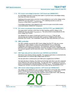
7.8 HBC controller
The HBC controller converts the 400 V boost voltage from the PFC into one or more
regulated DC output voltages. It drives two external MOSFETS in a half-bridge
configuration connected to a transformer. The transformer, which has a leakage
inductance and a magnetizing inductance, forms the resonant circuit in combination with
the resonant capacitor and the load at the output. The regulation is realized via frequency
control.
7.8.1 HBC high-side and low-side driver (pin GATEHS and GATELS)
Both drivers have identical driving capability. The output of each driver is connected to the
equivalent gate of an external high-voltage power MOSFET.
The low-side driver is referenced to pin PGND and is supplied from SUPREG.
The high-side driver is floating. The reference for the high-side driver is pin HB, connected
to the midpoint of the external half-bridge. The high-side driver is supplied from SUPHS
which is connected to the external bootstrap capacitor CSUPHS. The bootstrap capacitor is
charged from SUPREG via external diode DSUPHS when the low-side MOSFET is on.
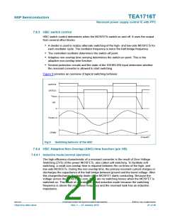
7.8.2 HBC boost undervoltage protection, UVP-boost (pin SNSBOOST)
The voltage on the SNSBOOST pin is sensed continuously to prevent the HBC controller
trying to operate at very low boost input voltages. Once VSNSBOOST drops below
V
uvp(SNSBOOST), HBC switching stops the next time GATELS goes HIGH. HBC switching
resumes as soon as VSNSBOOST rises above Vstart(SNSBOOST).
TEA1716T
All information provided in this document is subject to legal disclaimers.
© NXP B.V. 2012. All rights reserved.
Objective data sheet
Rev. 1 — 27 January 2012
20 of 46

 ETC [ ETC ]