TEA1716T
NXP Semiconductors
Resonant power supply control IC with PFC
The PFC controller uses valley switching to minimize losses. A primary stroke is only
started once the previous secondary stroke has ended and the voltage across the PFC
MOSFET has reached a minimum value.
7.7.1 PFC gate driver (pin GATEPFC)
The circuit driving the gate of the power MOSFET has a high current sourcing capability
Isource(GATEPFC) (500 mA typical) and a high current sink capability Isink(GATEPFC)
(1.2 A typical). This permits fast turn-on and turn-off of the power MOSFET to ensure
efficient operation. The driver is supplied from the regulated SUPREG supply.
7.7.2 PFC on-time control
The PFC operates under on-time control. The on-time of the PFC MOSFET is determined
by:
• The error amplifier and the loop compensation via the voltage on pin COMPPFC
At Vton(COMPPFC)zero (3.5 V typical), the on-time is reduced to zero. At Vton(COMPPFC)max
the on-time is at a maximum
• Mains compensation via the voltage on pin SNSMAINS
7.7.2.1 PFC error amplifier (pins COMPPFC and SNSBOOST)
The boost voltage is divided via a high-ohmic resistive divider. It is fed to the SNSBOOST
pin. The transconductance error amplifier, which compares the SNSBOOST voltage with
an accurate trimmed reference voltage Vreg(SNSBOOST), is connected to this pin. The
external loop compensation network at the COMPPFC pin filters the output current. In a
typical application, a resistor and two capacitors set the bandwidth of the regulation loop.
The transconductance of the error amplifier is not constant. This improves the start-up
behavior and transient response. The transconductance significantly increases resulting
in a higher output current to pin COMPPFC when the SNSBOOST voltage is more than
80 mV above or below the reference voltage.
The COMPPFC voltage is clamped at a maximum of Vclamp(COMPPFC). This avoids a long
recovery time if the boost voltage rises above the regulation level for a certain period.
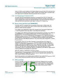
7.7.2.2 PFC mains compensation (pin SNSMAINS)
The mathematical equation for the transfer function of a power factor corrector contains
the square of the mains input voltage. In a typical application, this results in a low
bandwidth for low mains input voltages, while at high mains input voltages the MHR
requirements can be hard to meet.
The TEA1716 contains a correction circuit to compensate for this effect. The average
mains voltage is measured via the SNSMAINS pin and this information is fed to an
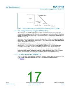
internal compensation circuit. Figure 7 illustrates the relationship between the SNSMAINS
voltage, the COMPPFC voltage, and the on-time. This compensation makes it is possible
to keep the regulation loop bandwidth constant over the full mains input range. This yields
a fast transient response on load steps, while still complying with class-D MHR
requirements.
TEA1716T
All information provided in this document is subject to legal disclaimers.
© NXP B.V. 2012. All rights reserved.
Objective data sheet
Rev. 1 — 27 January 2012
16 of 46

 ETC [ ETC ]