Ver 1.3
PRELIMINARY
EAGLE
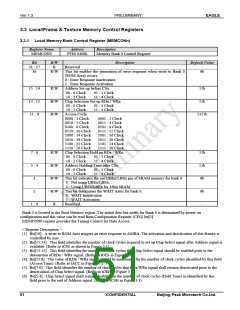
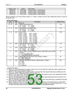
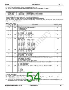
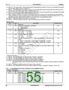
3.3 Local/Frame & Texture Memory Control Registers
3.3.1 Local Memory Bank Control Register (MEMCONn)
Register Name
Address
Description
MEMCON0
FFE0 0400h
Memory Bank 0 Control Register
Bit
31 : 17
16
R/W
R
R/W
Description
Default Value
Reserved
-
0b
This bit enables the generation of error response when write to Bank 0
(ROM Area) occurs.
0 : Error Response Inactivation
1 : Error Response Activation
15 : 14
13 : 12
11 : 8
R/W
R/W
R/W
Address Set-up before CSx
11b
11b
00 : 0 Clock
10 : 2 Clock
01 : 1 Clock
11 : 4 Clock
Chip Selection Set-up RDx / WRx
00 : 0 Clock
10 : 2 Clock
01 : 1 Clock
11 : 4 Clock
Access Cycle
0000 : 1 Clock
0010 : 3 Clock
0100 : 6 Clock
0110 : 10 Clock
1000 : 14 Clock
1010 : 18 Clock
1100 : 22 Clock
1110 : 26 Clock
1111b
0001 : 2 Clock
0011 : 4 Clock
0101 : 8 Clock
0111 : 12 Clock
1001 : 16 Clock
1011 : 20 Clock
1101 : 24 Clock
1111 : 30 Clock
7 : 6
5 : 4
3
R/W
R/W
R/W
R/W
R
Chip Selection Hold on RDx / WRx
11b
11b
0b
0b
-
00 : 0 Clock
10 : 2 Clock
01 : 1 Clock
11 : 4 Clock
Address Holding Time after CSx
00 : 0 Clock
10 : 2 Clock
01 : 1 Clock
11 : 4 Clock
This bit indicates the use UBEx/LBEx pin of SRAM memory for bank 0
0 : Not using UBEx/LBEx
1 : Using UBEx/LBEx for 16bit SRAM
This bit determines the WAIT status for bank 0.
0 : WAIT Inactivation
1 : WAIT Activation
Reserved
2
1 : 0
Bank 0 is located in the Boot Memory region. The initial data bus width for Bank 0 is determined by power on
configuration and this value can be read from Configuration Register (CFG) bit[5].
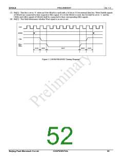
MEMCON0 register provides the Timing Control for Data Access.
< Register Description >
(1) Bit[16] : A write to ROM Area triggers an error response to AMBA. The activation and deactivation of this feature is
controlled by user.
(2) Bit[15:14] : This field identifies the number of clock cycles required to set up Chip Select signal after Address signal is
available. (Refer to tCSS as shown in Figure 3.1)
(3) Bit[13:12] : This field identifies the number of clock cycles that Chip Select signal should be enabled prior to the
deassertion of RDx / WRx signal. (Refer to tOES in Figure 3.1)
(4) Bit[11:8] : The value of RDx / WRx signal should be maintained for the number of clock cycles identified by this field
(Access Time). (Refer to tACC in Figure 3.1)
(5) Bit[7:6] : This field identifies the number of clock cycles that RDx/WRx signal shall remain deactivated prior to the
deactivation of Chip Select signal. (Refer to tOEH in Figure 3.1)
(6) Bit[5:4] : Chip Select signal shall remain disabled for the number of clock cycles (Hold Time) as identified by this
field prior to the end of Address signal. (Refer to tCSH in Figure 3.1)
51
CONFIDENTIAL
Beijing Peak Microtech Co.Ltd.

 ETC [ ETC ]