Ver 1.3
PRELIMINARY
EAGLE
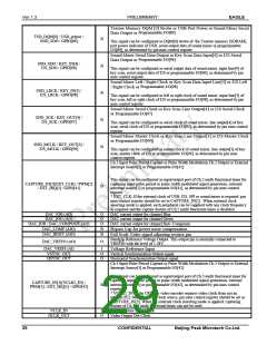
Texture Memory DQM [0] Strobe or USB Port Power or Sound Mixer Serial
Programmable I/O[89]
Data Output or
TSD_DQM[0] / USB_prtpwr /
B
B
B
B
B
SND_SDO / GPIO[89]
This signal can be configured as DQM[0] strobe of the Texture memory (SDRAM),
port power indicator of USB, serial output data of sound mixer or programmable
I/O[89], as determined by pin mux control register.
Sound Mixer Serial Data Output or Key Scan Data Input[4] or I2S Serial
Programmable I/O[96]
Data Output or
SND_SDO / KEY_IN[4] /
I2S_SDO / GPIO[96]
This signal can be configured as serial output data of sound mixer, input line[4] of
key scan, serial output data of I2S or programmable I/O[96], as determined by pin
mux control register.
Sound Mixer Left / Right Clock or Key Scan Data Input Line[3] or I2S Left
Programmable I/O[98]
/ Right Clock or
SND_LRCK / KEY_IN[3] /
I2S_LRCK / GPIO[98]
This signal can be configured as left or right clock of sound mixer, input line[3] of
key scan, left or right clock of I2S or programmable I/O[98], as determined by pin
mux control register.
Sound Mixer Serial Clock or Key Scan Line Output[4] or I2S Serial Clock
Programmable I/O[97]
or
SND_SCK / KEY_OUT[4] /
I2S_SCK / GPIO[97]
This signal can be configured as serial clock of sound mixer, line output[4] of key
scan, serial clock of I2S or programmable I/O[97], as determined by pin mux control
register.
Sound Mixer Master Clock or Key Scan Line Output[3] or I2S Master Clock
Programmable I/O[99]]
or
SND_MCLK / KEY_OUT[3] /
I2S_MCLK / GPIO[99]
This signal can be configured as master clock of sound mixer, line output[3] of key
scan, master clock of I2S or programmable I/O[99], as determined by pin mux
control register.
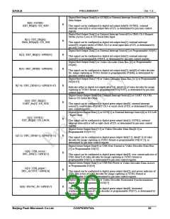
Ch.2 Input Pulse Period Capture or Pulse Width Modulation Ch.2 Output or External
Interrupt Source[2] or Programmable I/O[41]
This signal can be configured as input/output port of Ch.2 multi functional timer for
capturing input pulse period or pulse width modulated signal generation, external
interrupt source[2] or programmable I/O[41], as determined by pin mux control
register.
CAPTURE_IN[2](EXT_CLK) / PWM[2]
/ EXT_IRQ[2] / GPIO[41]
B
* EXT_CLK: If the external clock of USB, I2S, SPI or sound mixer is required, pin
mux control register should be set to CAPTURE_IN[2] . When external clock
asserting mode is applied, each peripheral can be supplied with any clock frequency
as required and the capture feature of Ch.2 multi functional timer is disabled.
DAC_IOB (AO)
DAC_IOG (AO)
DAC_IOR / DAC_COMPOSIT (AO)
DAC_COMP (AIO)
O
O
O
B
B
DAC current output for channel Blue
DAC current output for channel Green
DAC current output for channel Red / Composite
Bypass Cap for power noise compensation
Full Scale Video signal adjusting resistor pin
DAC_IRSET (AIO)
Bandgap Reference Voltage Output. This output pin is normally connected to
VREFIN with the level of 1.28V.
DAC_VREFO (AO)
O
DAC_VREFI (AI)
VSYNC_OUT
HSYNC_OUT
I
Voltage Reference Input
Vertical Synchronization Output signal.
Horizontal Synchronization Output signal.
O
O
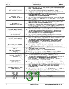
Ch.3 Input Pulse Period Capture or Pulse Width Modulation Ch.3 Output or External
Interrupt Source[3] or Programmable I/O[42]
This signal can be configured as input/output port of Ch.3 multi functional timer for
capturing input pulse period or pulse width modulated signal generation, external
interrupt source[3] or programmable I/O[42], as determined by pin mux control
register.
CAPTURE_IN[3](VCLK2_IN) /
PWM[3] / EXT_IRQ[3] / GPIO[42]
B
* VCLK2_IN: If the CRTC or video encoder requires video clock from not an
internal PLL but an external clock source, pin mux control register should be set as
CAPTURE_IN[3]. When the external clock asserting mode is applied, capturing
feature of Ch.3 of multi functional timer can not be used.
VCLK_IN
DCLK_OUT
I
O
Video Capture Input Clock
Video Output Dot Clock
29
CONFIDENTIAL
Beijing Peak Microtech Co.Ltd.

 ETC [ ETC ]