Ver 1.3
PRELIMINARY
EAGLE
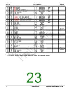
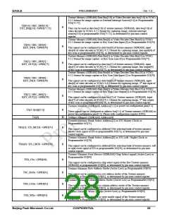
[6:4] or Power On Configuration pins[6:4]
Texture Memory (SDRAM) Address
TA[6:4](cfg[6:4])
B
They can be used as address[6:4] of texture memory (SDRAM), or power on
configuration pins[6:4]. Refer to Configuration Register (CFG).
TA[6] should be pull down to ground by 4.7K resistor.
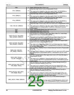
Texture Memory Clock or USB Over-Current or Sound Mixer Master Clock
Programmable I/O[88]
or
TSD_CLK / USB_ovrcur /
SND_MCLK / GPIO[88]
B
B
B
This signal can be configured as clock signal for texture memory (SDRAM), over
current indicator of USB, master clock of sound mixer or programmable I/O[88], as
determined by pin mux control register.
Programmable I/O[90]
Texture Memory (SDRAM) DQM [1] Strobe or
TSD_DQM[1] / GPIO[90]
This signal can be configured as DQM strobe[1] of texture memory (SDRAM) or
programmable I/O[90], as determined by pin mux control register.
Texture Memory (SDRAM) Data Bus[8] or Video Decoder Data Active Input signal
or Key Scan Data Input[2] or Programmable I/O[80]
TD[8] / DEC_ACTIVE /
KEY_IN[2] / GPIO[80]
This signal can be configured as Data bus[8] of texture memory (SDRAM), data
active signal of video decoder for capturing image, data input[2] of key scan or
programmable I/O[80], as determined by pin mux control register.
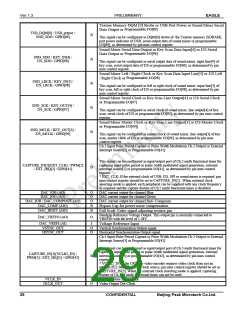
Texture Memory (SDRAM) Data Bus[9] or Video Decoder Horizontal
Synchronization Input signal or Key Scan Line Output[2] or Programmable I/O[81]
TD[9] / HSYNC_IN /
KEY_OUT[2] / GPIO[81]
B
B
B
B
B
B
B
This signal can be configured as data bus[9] of texture memory (SDRAM),
horizontal synchronization signal of video decoder, line output[2] of key scan or
programmable I/O[81], as determined by pin mux control register.
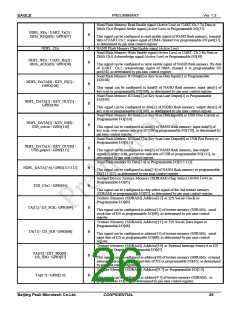
Texture Memory (SDRAM) Data Bus[10] or Video Decoder Vertical
Synchronization Input or Key Scan Data Input[1] or Programmable I/O[82]
TD[10] / VYSNC_IN /
KEY_IN[1] / GPIO[82]
This signal can be configured as data bus[10] of texture memory (SDRAM), vertical
synchronization signal of video decoder, data input[1] of key scan or programmable
I/O[82], as determined by pin mux control register.
Texture Memory (SDRAM) Data Bus[11] or Video Decoder Field Input Indicator or
Key Scan Line Output[1] or Programmable I/O[83]
TD[11] / DEC_FIELD /
KEY_OUT[1] / GPIO[83]
This signal can be configured as d Data bus[11] of texture memory (SDRAM), field
input indicator of video decoder for capturing image, line output[1] of key scan or
programmable I/O[83], as determined by pin mux control register.
Texture Memory (SDRAM) Data Bus[12] or UART Ch.2 Tx Data or Key Scan Data
Input[0] or Programmable I/O[84]
TD[12] / UART_Tx[2] /
KEY_IN[0] / GPIO[84]
This signal can be configured as data bus[12] of texture memory (SDRAM), Tx data
of UART Ch.2, line input[0] of key scan or programmable I/O[84], as determined by
pin mux control register.
Texture Memory (SDRAM) Data Bus[13] or UART Ch.2 Rx Data or Key Scan Line
Output[0] or Programmable I/O[85]
TD[13] / UART_Rx[2] /
KEY_OUT[0] / GPIO[85]
This signal can be configured as data bus[13] texture memory (SDRAM), receive
data of UART Ch.2, line output[0] of key scan or programmable I/O[85], as
determined by pin mux control register.
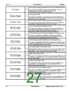
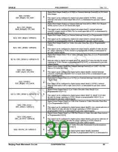
Texture Memory (SDRAM) Data Bus[14] or External Interrupt Source[1] or Sound
Mixer Serial Bit Clock or Programmable I/O[86]]
TD[14] / EXT_IRQ[1] /
SND_SCK / GPIO[86]
This signal can be configured as data bus[14] of texture memory (SDRAM), external
interrupt source[1], serial clock of sound mixer or programmable I/O[86], as
determined by pin mux control register.
Texture Memory (SDRAM) Data Bus[15] or External Interrupt Source[3] or Sound
Mixer Left / Right Clock or Programmable I/O[87]
TD[15] / EXT_IRQ[3] /
SND_LRCK /GPIO[87]
This signal can be configured as data bus[15] of texture memory (SDRAM), external
interrupt source[3], left of right clock of sound mixer or programmable I/O[87], as
determined by pin mux control register.
27
CONFIDENTIAL
Beijing Peak Microtech Co.Ltd.

 ETC [ ETC ]