EAGLE
PRELIMINARY
Ver 1.3
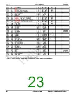
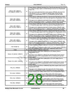
Nand Flash Memory Read Enable signal (Active Low) or UART Ch.2 Tx Data or
DMA Ch.0 Request Strobe signal (Active Low) or Programmable I/O[37]
NDFL_REx / UART_Tx[2] /
DMA_REQx[0] / GPIO[37]
B
O
B
This signal can be configured as read enable signal of NAND flash memory, transmit
data of UART Ch.2, request signal of DMA channel 0 or programmable I/O port[37],
as determined by pin mux control register.
NAND Flash Memory Chip Enable signal (Active Low)
Nand Flash Memory Write Enable signal (Active Low) or UART Ch.2 Rx Data or
DMA Ch.0 Acknowledge signal (Active Low) or Programmable I/O[38]
NDFL_CEx
NDFL_WEx / UART_Rx[2] /
DMA_ACKx[0] / GPIO[38]
This signal can be configured as write enable signal of NAND flash memory, Rx data
of UART Ch.2, acknowledge signal of DMA channel 0 or programmable I/O
port[38], as determined by pin mux control register.
Nand Flash Memory IO Data[0] or Key Scan Data Input[1] or Programmable
I/O[108]
NDFL_DATA[0] / KEY_IN[1] /
GPIO[108]
B
B
This signal can be configured as data[0] of NAND flash memory, input data[1] of
key scan or programmable I/O[108], as determined by pin mux control register.
Nand Flash Memory IO Data[1] or Key Scan Line Output[1] or Programmable
I/O[109]
NDFL_DATA[1] / KEY_OUT[1] /
GPIO[109]
This signal can be configured as data[1] of NAND flash memory, output data[1] of
key scan or programmable I/O[109], as determined by pin mux control register
Nand Flash Memory IO Data[2] or Key Scan Data Input[0] or USB Over-Current or
Programmable I/O[110]
NDFL_DATA[2] / KEY_IN[0] /
USB_ovrcur / GPIO[110]
B
B
This signal can be configured as data[2] of NAND flash memory, input data[0] of
key scan, over current indicator of USB or programmable I/O[110], as determined by
pin mux control register.
Nand Flash Memory IO Data[3] or Key Scan Line Output[0] or USB Port Power or
Programmable I/O[111]]
NDFL_DATA[3] / KEY_OUT[0] /
USB_prtpwr / GPIO[111]
This signal can be configured as data[3] of NAND flash memory, line output
signal[0] of key scan, port power indicator of USB or programmable I/O[111], as
determined by pin mux control register.
Nand Flash memory IO Data[7:4] or Programmable I/O[115:112]
NDFL_DATA[7:4] / GPIO[115:112]
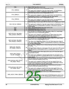
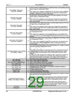
TSD_CSx2 / GPIO[95]
B
B
This signal can be configured as data[7:4] of NAND flash memory or programmable
I/O[115:112], as determined by pin mux control register.
(Active Low)
Second Device Texture Memory (SDRAM) Chip Select
Programmable I/O[95]
or
This signal can be configured as chip select signal of the 2nd texture memory
(SDRAM) or programmable I/O[95], as determined by pin mux control register.
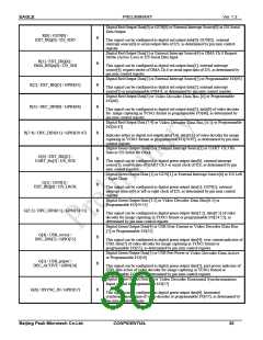
Texture Memory (SDRAM) Address[12] or I2S Serial Clock or
Programmable I/O[69]
TA[12] / I2S_SCK / GPIO[69]
TA[11] / I2S_SDI / GPIO[68]
B
B
This signal can be configured as address[12] of texture memory (SDRAM), serial
clock line of I2S or programmable I/O[69], as determined by pin mux control
register.
Texture Memory (SDRAM) Address[11] or I2S Serial Data Input or
Programmable I/O[68]
This signal can be configured as address[11] of texture memory (SDRAM), serial
input data of I2S or programmable I/O[68], as determined by pin mux control
register.
External Interrupt Source 0 or I2S
Texture Memory (SDRAM) Address[10] or
Serial Data Output or Programmable I/O[67]
TA[10] / EXT_IRQ[0] /
I2S_SDO / GPIO[67]
B
B
This signal can be configured as address[10] of texture memory (SDRAM), external
interrupt source[0], serial output data of I2S or programmable I/O[67], as determined
by pin mux control register.
Programmable I/O[2:0]
Texture Memory (SDRAM) Address[9:7] or
TA[9:7] / GPIO[2:0]
This signal can be configured as address[9:7] of texture memory (SDRAM), or
programmable I/O[2:0], as determined by pin mux control register.
Beijing Peak Microtech Co.Ltd.
CONFIDENTIAL
26

 ETC [ ETC ]