Ver 1.3
PRELIMINARY
EAGLE
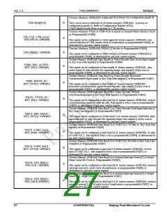
Digital Green Output Data [7] or
Video Decoder Vertical Synchronization Input
or Programmable I/O[58]
signal
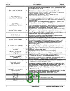
G[7] / VSYNC_IN / GPIO[58]
B
B
B
This signal can be configured as digital green Output Data[7], vertical
synchronization signal of v Programmable
I/O[58] as determined by pin mux control register.
ideo Decoder for image capturing or
Digital Blue Output Data[0] or UART Ch.3 Tx
Acknowledge(Active Low) or I2S Master Clock
or DMA Ch.0
Data
B[0] / UART_Tx[3] /
DMA_ACKx[0] / I2S_MCLK
This signal can be configured as digital blue output data[0], Transmit data of UART
Ch.3, acknowledge signal of DMA Ch.0 or master clock of I2S, as determined by pin
mux control register.
Digital Blue Output Data[1] or
or
Pulse Width Modulation Ch.1 Output Ch.1
Input
Programmable I/O[60]
Pulse Period Capture or
B[1] / PWM[1] /
CAPTURE_IN[1] / GPIO[60]
It can be used as digital blue output data[1], input/output port of ch.1 multi functional
timer for capturing input pulse period or pulse width modulated signal generation or
programmable I/O[60], as determined by pin mux control register.
Digital Blue Output Data[2] or External Interrupt Source 7 or Programmable I/O[61]
B[2] / EXT_IRQ[7] / GPIO[61]
B[5:3] / GPIO[64:62]
B
B
B
This signal can be configured as digital blue output data[2], external interrupt
source[7] or programmable I/O[61], as determined by pin mux control register.
Digital Blue Output Data[5:3] or Programmable I/O[64:62]
This signal can be configured as digital blue output data[5:3] or programmable
I/O[64:62], as determined by pin mux control register.
Digital blue Output Data[6] or Video Decoder Field signal or Programmable I/O[65]
B[6] / DEC_FIELD / GPIO[65]
This signal can be configured as digital blue output data[6], field signal of video
decoder or programmable I/O[65], as determined by pin mux control register.
Digital Blue Output Data[7] or Composite Signal Synchronization Output or
Programmable I/O[66]
B[7] / CSYNC_OUT / GPIO[66]
DISP_EN
B
This signal can be configured as digital blue output data[7], synchronization output
of composite signal or programmable I/O[66], as determined by pin mux control
register.
RGB(Digital / Analog) Display Enable
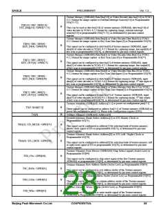
TWI Serial Data or UART Ch.3 Tx or Programmable I/O[106]
O
B
TWI_SDA / UART_Tx[3] /
GPIO[106]
This signal can be configured as serial data of TWI, transmit data of UART Ch.3 or
programmable I/O[106], as determined by pin mux control register.
TWI Serial Clock or UART Ch.3 Rx Data or Programmable I/O[107]
TWI_SCL / UART_Rx[3] /
GPIO[107]
B
B
This signal can be configured as serial clock of TWI, receive data of UART Ch.3 or
programmable I/O[107], as determined by pin mux control register.
UART Ch.1 Tx Data or Pulse Width Modulation Ch.0 Output or On Silicon In
Circuit Emulator Tx Data or Programmable I/O[39]
UART_Tx[1] / PWM[0] /
OSI_Tx / GPIO[39]
This signal can be configured as transmit data of UART Ch.1, output port of Ch.0
multi functional timer for generating pulse width modulated signal, transmit data of
OSI or programmable I/O[39], as determined by pin mux control register.
UART Ch.1 Rx Data or
Programmable I/O[40]
Input
or OSI Rx or
Pulse Period Capture
Ch.0
UART_Rx[1] / CAPTURE_IN[0] /
OSI_Rx / GPIO[40]
B
This signal can be configured as receive data of UART Ch.1, input port of Ch.0 multi
functional timer for capturing input pulse period, receive data of OSI or
programmable I/O[40], as determined by pin mux control register.
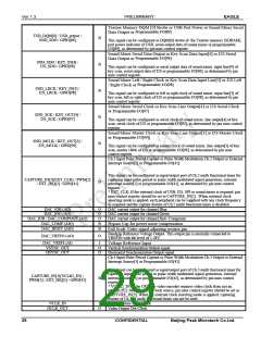
UART_Tx[0]
UART_Rx[0]
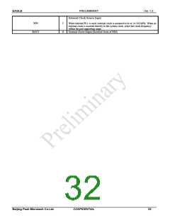
RTC_XIN
RTC_XOUT
USB_DN
O
I
I
O
B
B
UART Ch.0 Transmit Data
UART Ch.0 Receive Data
RTC External Clock Input
RTC External clock output (Inverted clock of RTC_XIN)
USB DN
USB_DP
USB DP
31
CONFIDENTIAL
Beijing Peak Microtech Co.Ltd.

 ETC [ ETC ]