EAGLE
PRELIMINARY
Ver 1.3
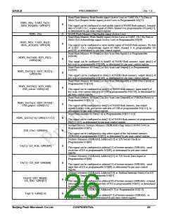
Texture Memory (SDRAM) Data Bus[3:0] or Video Decoder data bus[3:0] in YCbCr
4:2:2 format for image capture or External Interrupt Sources[3:0] or Programmable
I/Os[75:72]
TD[3:0] / DEC_DIN[3:0] /
EXT_IRQ[3:0] / GPIO[75:72]
B
They can be used as data bus[3:0] of texture memory (SDRAM), data bus[3:0] of
video decoder in YCbCr 4:2:2 format for capturing image, external interrupt
sources[3:0] or programmable I/Os[75:72], as determined by pin mux control
register.
Texture Memory (SDRAM) Data Bus[4] or Video Decoder Data Bus[4] in YCbCr
4:2:2 format for image capture or Key Scan Data Input [4] or Programmable I/O[76]
TD[4] / DEC_DIN[4] /
KEY_IN[4] / GPIO[76]
B
B
B
B
This signal can be configured as data bus[4] of texture memory (SDRAM), input
data[4] of video decoder in YCbCr 4:2:2 format for capturing image, line input[4] of
key scan or programmable I/O[76], as determined by pin mux control register.
Texture Memory (SDRAM) Data Bus[5] or Video Decoder Data Bus[5] in YCbCr
4:2:2 format for image capture or Key Scan Line [4] or Programmable I/O[77]
TD[5] / DEC_DIN[5] /
KEY_OUT[4] / GPIO[77]
This signal can be configured as data bus[5] of texture memory (SDRAM), input
data[5] of video decoder in YCbCr 4:2:2 format for capturing image, line output[4]
of key scan or programmable I/O[77], as determined by pin mux control register.
Texture Memory (SDRAM) Data Bus[6] or Video Decoder Data Bus [6] in YCbCr
4:2:2 format for image capture or Key Scan Data Input [3] or Programmable I/O[78]
TD[6] / DEC_DIN[6] /
KEY_IN[3] / GPIO[78]
This signal can be configured as data bus[6] of texture memory (SDRAM), input
data[6] of video decoder as YCbCr 4:2:2 format for capturing image, 3rd line input of
key scan or programmable I/O[78], as determined by pin mux control register.
Texture Memory (SDRAM) Data Bus[7] or Video Decoder Data Bus [7] in YCbCr
4:2:2 format for image capture or Key Scan Line Output[3] or Programmable I/O[79]
TD[7] / DEC_DIN[7] /
KEY_OUT[3] / GPIO[79]
This signal can be configured as data bus[7] of Texture memory (SDRAM), input
data[7] of video decoder as YCbCr 4:2:2 format for capturing image, 3rd line output
of key scan or programmable I/O[79], as determined by pin mux control register.
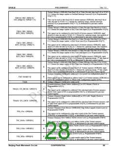
or power on configuration pins[3:1]
Texture Memory (SDRAM) Address[3:1]
TA[3:1](cfg[3:1])
TA[0]
B
B
These signals can be configured as address bus[3:1] of Texture memory (SDRAM) or
power on configuration pins[3:1]. Please refer configuration register (CFG).
Texture Memory (SDRAM) Address[0]
Texture Memory Bank Select Address[1] or I2S Master Clock or
Programmable I/O[71]
TBA[1] / I2S_MCLK / GPIO[71]
B
This signal can be configured as address[1] for selecting bank of texture memory,
master clock signal of I2S or programmable I/O[71], as determined by pin mux
control register.
Texture Memory Bank Select Address[0] or I2S Left / Right Clock or
Programmable I/O[70]
TBA[0] / I2S_LRCK / GPIO[70]
TSD_CSx / GPIO[94]
B
B
This signal can be configured as address[0] for selecting bank of texture memory, left
or right clock signal of I2S or programmable I/O[70], as determined by pin mux
control register.
(Active Low)
Texture Memory First Device (SDRAM) Chip Select signal
Programmable I/O[94]
or
This signal can be configured as chip select signal of the first Texture memory
(SDRAM) or programmable I/O[94], as determined by pin mux control register.
Row Address Strobe (Active Low) Programmable I/O[91]
Texture Memory
or
TSC_RASx / GPIO[91]
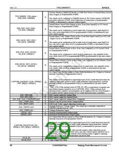
TSD_CASx / GPIO[92]
TSD_WEx / GPIO[93]
B
B
B
This signal can be configured as row address strobe of the Texture memory
(SDRAM) or Programmable I/O[91], as determined by pin mux control register.
Column Address Strobe (Active Low) Programmable I/O[92]
Texture Memory
or
This signal can be configured as column address strobe of the Texture memory
(SDRAM) or Programmable I/O[92], as determined by pin mux control register.
(Active Low) Programmable I/O[93]
Texture Memory Write Enable
or
This signal can be configured as write enable signal of the Texture memory
(SDRAM) or Programmable I/O[93], as determined by pin mux control register
Beijing Peak Microtech Co.Ltd.
CONFIDENTIAL
28

 ETC [ ETC ]