EAGLE
PRELIMINARY
Ver 1.3
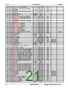
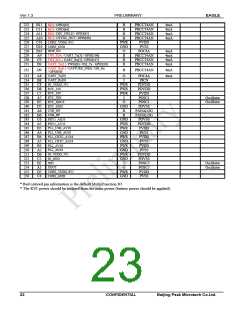
2.4 Pin Description
Description
Pin name
I/O
Indicates set up as Chip Test Mode. (Active High)
For normal mode, TEST pin should be set to 0.
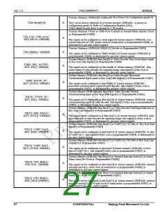
TEST
I
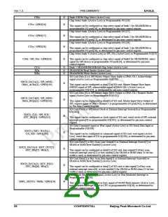
RESETx
TRST
I
I
System Chip Reset (Active Low)
TRST for JTAG Interface
TDI
I
TDI for JTAG Interface
TCK
I
TCK for JTAG Interface
TMS
I
TMS for JTAG Interface
TDO
O
B
O
O
O
O
O
O
TDO for JTAG Interface
Local ROM/SRAM/SDRAM Data Bus[31:0]
Local SDRAM DQM Strobes
D[31:0]
SD_DQM[3:0]
SD_CLK
CS6x
SD_RASx
SD_CASx
SD_WEx
Local SDRAM Clock
Bank 6 SRAM/ROM/SDRAM Chip Select (Active Low)
Local SDRAM Row Address Strobe (Active Low)
Local SDRAM Column Address Strobe (Active Low)
Local SDRAM Write Enable (Active Low)
Address[0] or Byte Enable[0] of SRAM or ROM (Active Low)
A[0](BEx[0])
O
When data bus width is 32 or 16 bits, this signal is byte enable bit[0]. When data bus
width is 8 bits, this pin can be configured as address bit[0].
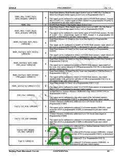
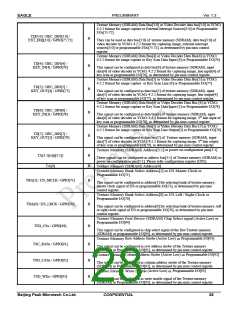
Address[13:1] (RAM Address[12:0])
A[13:1] (RA[12:0])
A[14]
O
O
O
These signals can be configured either as address bits[13:1] or RA[12:0] to indicate
address bits[12:0] of SRAM, ROM.
Address[14]
Address[16:15] (Bank select Address[1:0])
A[16:15](BA[1:0])
These signals can be configured either as address bits[16:15] or BA[1:0] to indicate
bank select address bits in SDRAM.
Byte Enable[1] of SRAM, ROM. (Active Low) or External Interrupt Source[2] or
Programmable I/O[15]
BEx[1] / EXT_IRQ[2] / GPIO[15]
B
When data bus width is 32 or 16 bits, this signal is used either as byte enable bit[1],
external interrupt source[2] or programmable I/O[15], as determined by pin mux
control register.
Address[19:17] or Programmable I/O[8:6]
A[19:17] / GPIO[8:6]
B
B
These signals can be configured as address bits[19:17] or programmable I/O
port[8:6], as determined by pin mux control register.
Address[21:20] or External Interrupt Sources[7:6] or Programmable I/Os[10:9]
A[21:20] / EXT_IRQ[7:6] / GPIO[10:9]
These signals can be configured as address bits[21:20], external interrupt
sources[7:6] or programmable I/O ports[10:9], as determined by pin mux control
register.
Address[23:22] or GUN[1:0] or External Interrupt Sources[5:4] or Programmable
I/Os[12:11]
A[23:22] / GUN[1:0] /
EXT_IRQ[5:4] / GPIO[12:11]
B
B
B
These signals can be configured as address bits[23:22], GUN[1:0], external interrupt
sources[5:4] or programmable I/O ports[12:11], as determined by pin mux control
register.
Nand Flash memory Address Latch Enable or Address [24] or Programmable I/O[13]
NDFL_ALE / A[24] / GPIO[13]
NDFL_CLE / A[25] / GPIO[14]
This signal can be configured as address latch enable signal of NAND flash memory,
address bit[24] or programmable I/O port[13], as determined by pin mux control
register.
Nand Flash memory Command Latch Enable or Address [25] or Programmable
I/O[14]
This signal can be configured as command latch enable signal of NAND flash
memory, address bit[25] or programmable I/O port[14], as determined by pin mux
control register.
Beijing Peak Microtech Co.Ltd.
CONFIDENTIAL
24

 ETC [ ETC ]