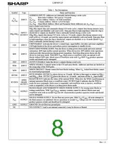
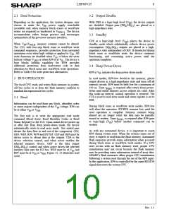
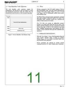
LHF80V25
10
sharp
(1,2)
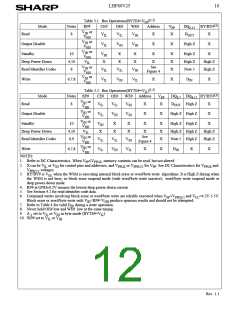
Table 3.1. Bus Operations(BYTE#=V )
IH
(3)
Mode
Read
Notes
8
RP#
or
CE#
OE#
WE#
Address
V
DQ
D
RY/BY#
X
PP
0-15
V
IH
V
V
V
X
X
IL
IL
IH
OUT
V
HH
V
V
or
IH
Output Disable
V
V
V
X
X
High Z
X
X
IL
IH
IH
HH
or
V
V
IH
Standby
10
4,10
8
V
X
X
X
X
X
X
X
X
X
High Z
High Z
Note 5
IH
HH
Deep Power-Down
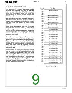
Read Identifier Codes
V
X
High Z
High Z
IL
or
V
V
See
Figure 4
IH
V
V
V
IL
IL
IH
HH
V
V
or
IH
Write
6,7,8
V
V
V
X
X
D
X
IL
IH
IL
IN
HH
(1,2)
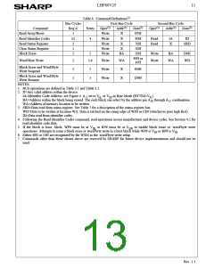
Table 3.2. Bus Operations(BYTE#=V )
IL
(3)
Mode
Read
Notes
8
RP#
or
CE#
OE#
WE# Address
V
DQ
D
DQ
RY/BY#
High Z X
PP
0-7
8-15
V
IH
V
V
V
X
X
X
IL
IL
IH
IH
OUT
V
HH
V
V
or
IH
Output Disable
V
V
V
X
High Z High Z
X
IL
IH
HH
V
V
or
IH
Standby
10
4,10
8,9
V
X
X
X
X
X
X
X
X
High Z High Z
High Z High Z
Note 5 High Z
X
IH
HH
Deep Power-Down
Read Identifier Codes
V
X
X
High Z
High Z
IL
or
V
V
See
Figure 4
IH
V
V
V
IH
IL
IL
HH
V
V
or
IH
Write
6,7,8
V
V
V
X
X
D
IN
X
X
IL
IH
IL
HH
NOTES:
1. Refer to DC Characteristics. When V ≤V
, memory contents can be read, but not altered.
PP
PPLK
2. X can be V or V for control pins and addresses, and V
or V
for V . See DC Characteristics for V
and
IL
IH
PPLK
PPH1/2
PP
PPLK
V
voltages.
PPH1/2
3. RY/BY# is V when the WSM is executing internal block erase or word/byte write algorithms. It is High Z during when
OL
the WSM is not busy, in block erase suspend mode (with word/byte write inactive), word/byte write suspend mode or
deep power-down mode.
4. RP# at GND±0.2V ensures the lowest deep power-down current.
5. See Section 4.2 for read identifier code data.
6. Command writes involving block erase or word/byte write are reliably executed when V =V
and V =4.5V-5.5V.
CC
PP
PPH1/2
Block erase or word/byte write with V <RP#<V produce spurious results and should not be attempted.
IH
HH
7. Refer to Table 4 for valid D during a write operation.
IN
8. Never hold OE# low and WE# low at the same timing.
9.
A
set to V or V in byte mode (BYTE#=V ).
-1
IL
IL
IH
IH
IL
10. WP# set to V or V .
Rev. 1.1

 ETC [ ETC ]