LHF80V25
7
sharp
2 PRINCIPLES OF OPERATION
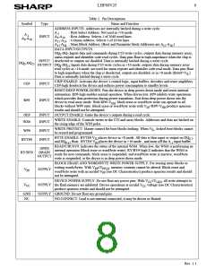
[A18-A0]
Top Boot
The LH28F800BVE-TV85 Smart5 Flash memory includes
an on-chip WSM to manage block erase and word/byte
write functions. It allows for: 100% TTL-level control
inputs, fixed power supplies during block erasure and
word/byte write, and minimal processor overhead with
RAM-like interface timings.
7FFFF
4K-word Boot Block
0
1
7F000
7EFFF
4K-word Boot Block
7E000
7DFFF
4K-word Parameter Block
4K-word Parameter Block
4K-word Parameter Block
4K-word Parameter Block
4K-word Parameter Block
4K-word Parameter Block
32K-word Main Block
32K-word Main Block
32K-word Main Block
32K-word Main Block
32K-word Main Block
32K-word Main Block
32K-word Main Block
32K-word Main Block
32K-word Main Block
32K-word Main Block
32K-word Main Block
32K-word Main Block
32K-word Main Block
32K-word Main Block
32K-word Main Block
0
7D000
7CFFF
1
7C000
7BFFF
After initial device power-up or return from deep power-
down mode (see Bus Operations), the device defaults to
read array mode. Manipulation of external memory control
pins allow array read, standby and output disable
operations.
2
7B000
7AFFF
3
7A000
79FFF
4
79000
78FFF
Status register and identifier codes can be accessed
5
through the CUI independent of the V voltage. High
78000
77FFF
PP
voltage on V
enables successful block erasure and
PP
0
70000
6FFFF
word/byte writing. All functions associated with altering
memory contents−block erase, word/byte write, status and
identifier codes−are accessed via the CUI and verified
through the status register.
1
68000
67FFF
2
60000
5FFFF
3
Commands are written using standard microprocessor
write timings. The CUI contents serve as input to the
WSM, which controls the block erase and word/byte write.
The internal algorithms are regulated by the WSM,
including pulse repetition, internal verification and
margining of data. Addresses and data are internally latch
during write cycles. Writing the appropriate command
outputs array data, accesses the identifier codes or outputs
status register data.
58000
57FFF
4
50000
4FFFF
5
48000
47FFF
6
40000
3FFFF
7
38000
37FFF
8
30000
2FFFF
Interface software that initiates and polls progress of block
erase and word/byte write can be stored in any block. This
code is copied to and executed from system RAM during
flash memory updates. After successful completion, reads
are again possible via the Read Array command. Block
erase suspend allows system software to suspend a block
erase to read/write data from/to blocks other than that
which is suspend. Word/byte write suspend allows system
software to suspend a word/byte write to read data from
any other flash memory array location.
9
28000
27FFF
10
11
12
13
14
20000
1FFFF
18000
17FFF
10000
0FFFF
08000
07FFF
00000
Figure 3. Memory Map
Rev. 1.1

 ETC [ ETC ]