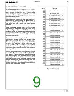
LHF80V25
6
sharp
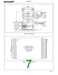
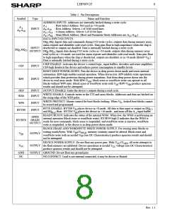
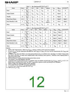
Table 2. Pin Descriptions
Symbol
Type
Name and Function
ADDRESS INPUTS: Addresses are internally latched during a write cycle.
A
: Byte Select Address. Not used in ×16 mode.
: Row Address. Selects 1 of 2048 word lines.
-1
A
-1
INPUT A -A
0
10
A -A
0
18
A -A : Column Address. Selects 1 of 16 bit lines.
11 14
A -A : Main Block Address. (Boot and Parameter block Addresses are A -A .)
15 18
12 18
DATA INPUT/OUTPUTS:
DQ -DQ :Inputs data and commands during CUI write cycles; outputs data during memory array,
0
7
status register and identifier code read cycles. Data pins float to high-impedance when the chip is
INPUT/ deselected or outputs are disabled. Data is internally latched during a write cycle.
DQ -DQ
0
15
OUTPUT DQ -DQ :Inputs data during CUI write cycles in ×16 mode; outputs data during memory array
8
15
read cycles in ×16 mode; not used for status register and identifier code read mode. Data pins float
to high-impedance when the chip is deselected, outputs are disabled, or in ×8 mode (Byte#=V ).
IL
Data is internally latched during a write cycle.
CHIP ENABLE: Activates the device’s control logic, input buffers, decoders and sense amplifiers.
CE#-high deselects the device and reduces power consumption to standby levels.
CE#
RP#
INPUT
INPUT
RESET/DEEP POWER-DOWN: Puts the device in deep power-down mode and resets internal
automation. RP#-high enables normal operation. When driven low, RP# inhibits write operations
which provides data protection during power transitions. Exit from deep power-down sets the
device to read array mode. With RP#=V , block erase or word/byte write can operate to all
HH
blocks without WP# state. Block erase or word/byte write with V <RP#<V produce spurious
IH
HH
results and should not be attempted.
OE#
INPUT OUTPUT ENABLE: Gates the device’s outputs during a read cycle.
WRITE ENABLE: Controls writes to the CUI and array blocks. Addresses and data are latched on
the rising edge of the WE# pulse.
WE#
INPUT
INPUT
INPUT
WRITE PROTECT: Master control for boot blocks locking. When V , locked boot blocks cannot
IL
WP#
be erased and programmed.
BYTE ENABLE: BYTE# V places device in ×8 mode. All data is then input or output on DQ
,
IL
0-7
BYTE#
and DQ
float. BYTE# V places the device in ×16 mode , and turns off the A input buffer.
8-15
IH -1
READY/BUSY#: Indicates the status of the internal WSM. When low, the WSM is performing an
internal operation (block erase or word/byte write). RY/BY#-high Z indicates that the WSM is
ready for new commands, block erase is suspended, and word/byte write is inactive, word/byte
write is suspended, or the device is in deep power-down mode.
OPEN
DRAIN
OUTPUT
RY/BY#
BLOCK ERASE AND WORD/BYTE WRITE POWER SUPPLY: For erasing array blocks or
writing words/bytes. With V ≤V
, memory contents cannot be altered. Block erase and
word/byte write with an invalid V (see DC Characteristics) produce spurious results and should
PP
PPLK
V
SUPPLY
PP
PP
not be attempted.
DEVICE POWER SUPPLY: Do not float any power pins. With V ≤V
, all write attempts to
CC
LKO
V
SUPPLY
the flash memory are inhibited. Device operations at invalid V voltage (see DC Characteristics)
CC
CC
produce spurious results and should not be attempted.
GND
NC
SUPPLY GROUND: Do not float any ground pins.
NO CONNECT: Lead is not internal connected; it may be driven or floated.
Rev. 1.1

 ETC [ ETC ]