LHF80V25
8
sharp
2.1 Data Protection
3.2 Output Disable
Depending on the application, the system designer may
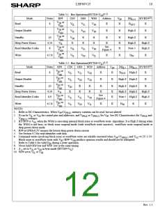
With OE# at a logic-high level (V ), the device outputs
IH
choose to make the V
power supply switchable
are disabled. Output pins (DQ -DQ ) are placed in a
PP
0
15
(available only when memory block erases or word/byte
writes are required) or hardwired to V . The device
high-impedance state.
PPH1/2
accommodates either design practice and encourages
optimization of the processor-memory interface.
3.3 Standby
CE# at a logic-high level (V ) places the device in
IH
When V ≤V
, memory contents cannot be altered.
standby mode which substantially reduces device power
consumption. DQ -DQ outputs are placed in a high-
PP
PPLK
The CUI, with two-step block erase or word/byte write
command sequences, provides protection from unwanted
0
15
impedance state independent of OE#. If deselected during
block erase or word/byte write, the device continues
functioning, and consuming active power until the
operation completes.
operations even when high voltage is applied to V . All
write functions are disabled when V is below the write
lockout voltage V
PP
CC
or when RP# is at V . The device’s
LKO
IL
boot blocks locking capability for WP# provides
additional protection from inadvertent code or data
alteration by block erase and word/byte write operations.
Refer to Table 6 for write protection alternatives.
3.4 Deep Power-Down
RP# at V initiates the deep power-down mode.
IL
In read modes, RP#-low deselects the memory, places
output drivers in a high-impedance state and turns off all
internal circuits. RP# must be held low for a minimum of
3 BUS OPERATION
The local CPU reads and writes flash memory in-system.
All bus cycles to or from the flash memory conform to
standard microprocessor bus cycles.
100 ns. Time t
is required after return from power-
PHQV
down until initial memory access outputs are valid. After
this wake-up interval, normal operation is restored. The
CUI is reset to read array mode and status register is set to
80H.
3.1 Read
Information can be read from any block, identifier codes
During block erase or word/byte write modes, RP#-low
will abort the operation. RY/BY# remains low until the
reset operation is complete. Memory contents being
altered are no longer valid; the data may be partially
or status register independent of the V voltage. RP# can
PP
be at either V or V
.
IH
HH
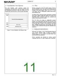
The first task is to write the appropriate read mode
command (Read Array, Read Identifier Codes or Read
Status Register) to the CUI. Upon initial device power-up
or after exit from deep power-down mode, the device
automatically resets to read array mode. Six control pins
dictate the data flow in and out of the component: CE#,
OE#, WE#, RP#, WP# and BYTE#. CE# and OE# must be
driven active to obtain data at the outputs. CE# is the
device selection control, and when active enables the
selected memory device. OE# is the data output
(DQ -DQ ) control and when active drives the selected
erased or written. Time t
is required after RP# goes
PHWL
to logic-high (V ) before another command can be
IH
written.
As with any automated device, it is important to assert
RP# during system reset. When the system comes out of
reset, it expects to read from the flash memory. Automated
flash memories provide status information when accessed
during block erase or word/byte write modes. If a CPU
reset occurs with no flash memory reset, proper CPU
initialization may not occur because the flash memory
may be providing status information instead of array data.
SHARP’s flash memories allow proper CPU initialization
following a system reset through the use of the RP# input.
In this application, RP# is controlled by the same RESET#
signal that resets the system CPU.
0
15
memory data onto the I/O bus. WE# must be at V and
IH
RP# must be at V or V . Figure 11, 12 illustrates read
IH
HH
cycle.
Rev. 1.1

 ETC [ ETC ]