LHF80V25
12
sharp
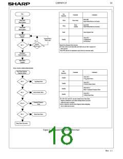
4.1 Read Array Command
4.4 Clear Status Register Command
Upon initial device power-up and after exit from deep
power-down mode, the device defaults to read array mode.
This operation is also initiated by writing the Read Array
command. The device remains enabled for reads until
another command is written. Once the internal WSM has
started a block erase or word/byte write, the device will
not recognize the Read Array command until the WSM
completes its operation unless the WSM is suspended via
an Erase Suspend or Word/Byte Write Suspend command.
The Read Array command functions independently of the
Status register bits SR.5, SR.4, SR.3 or SR.1 are set to
"1"s by the WSM and can only be reset by the Clear Status
Register command. These bits indicate various failure
conditions (see Table 7). By allowing system software to
reset these bits, several operations (such as cumulatively
erasing multiple blocks or writing several words/bytes in
sequence) may be performed. The status register may be
polled to determine if an error occurred during the
sequence.
To clear the status register, the Clear Status Register
command (50H) is written. It functions independently of
the applied V Voltage. RP# can be V or V . This
V
voltage and RP# can be V or V
.
PP
IH
HH
4.2 Read Identifier Codes Command
PP
IH
HH
command is not functional during block erase or
word/byte write suspend modes.
The identifier code operation is initiated by writing the
Read Identifier Codes command. Following the command
write, read cycles from addresses shown in Figure 4
retrieve the manufacturer and device codes (see Table 5
for identifier code values). To terminate the operation,
write another valid command. Like the Read Array
command, the Read Identifier Codes command functions
independently of the V voltage and RP# can be V or
4.5 Block Erase Command
Erase is executed one block at a time and initiated by a
two-cycle command. A block erase setup is first written,
followed by an block erase confirm. This command
sequence requires appropriate sequencing and an address
within the block to be erased (erase changes all block data
to FFFFH). Block preconditioning, erase, and verify are
handled internally by the WSM (invisible to the system).
After the two-cycle block erase sequence is written, the
device automatically outputs status register data when read
(see Figure 5). The CPU can detect block erase completion
by analyzing the output data of the RY/BY# pin or status
register bit SR.7.
PP
IH
V
. Following the Read Identifier Codes command, the
HH
following information can be read:
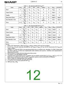
Table 5. Identifier Codes
Address
Data
Code
[A -A ] [DQ -DQ ]
18
0
7
0
Manufacture Code
Device Code
00000H
00001H
B0H
4CH
When the block erase is complete, status register bit SR.5
should be checked. If a block erase error is detected, the
status register should be cleared before system software
attempts corrective actions. The CUI remains in read
status register mode until a new command is issued.
4.3 Read Status Register Command
The status register may be read to determine when a block
erase or word/byte write is complete and whether the
operation completed successfully. It may be read at any
time by writing the Read Status Register command. After
writing this command, all subsequent read operations
output data from the status register until another valid
command is written. The status register contents are
latched on the falling edge of OE# or CE#, whichever
This two-step command sequence of set-up followed by
execution ensures that block contents are not accidentally
erased. An invalid Block Erase command sequence will
result in both status register bits SR.4 and SR.5 being set
to "1". Also, reliable block erasure can only occur when
V
=4.5V-5.5V and V =V
. In the absence of this
occurs. OE# or CE# must toggle to V before further
CC
PP
PPH1/2
IH
high voltage, block contents are protected against erasure.
reads to update the status register latch. The Read Status
If block erase is attempted while V ≤V , SR.3 and
Register command functions independently of the V
PP
PPLK
PP
SR.5 will be set to "1". Successful block erase for boot
blocks requires that the corresponding if set, that
WP#=V or RP#=V . If block erase is attempted to
voltage. RP# can be V or V
.
IH
HH
IH
HH
boot block when the corresponding WP#=V
or
IL
RP#=V , SR.1 and SR.5 will be set to "1". Block erase
IH
operations with V <RP#<V
produce spurious results
IH
HH
and should not be attempted.
Rev. 1.1

 ETC [ ETC ]