1-2-6 High Voltage 3-Phase Brushless Motor Driver ICs
SMA/SLA6820MP Series Built-in Thermal Sensor and 7.5 V Regulator
■Features
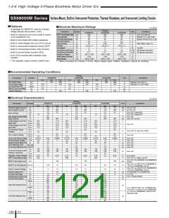
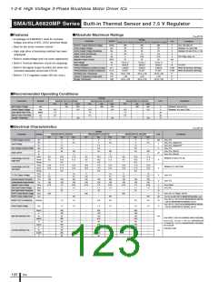
■Absolute Maximum Ratings
(Ta=25°C)
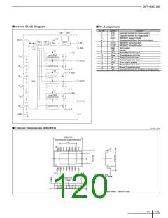
• A package of 6 MOSFET units for 3-phase
Ratings
Parameter
Symbol
Unit
Conditions
SMA6821MP/SLA6826M SMA6822MP/SLA6827M SMA6823MP/SLA6828M
bridge, pre-drive (HVIC, LVIC) and boot diode
MOSFET Output Withstand Voltage
Control Supply Voltage
VDSS
Vcc
250
20
500
20
500
20
V
V
Vcc=15V,VIN=0V
• Best for fan motor inverter control
Between VCC and COM
Control Supply Voltage (Bootstrap)
Output Current (continuous)
Output Current (pulse)
V
BS
20
20
20
V
Between VB and HS (U, V, W)
• High side drive of bootstrap method has been
employed.
Io
2.0
1.5
2.5
A
Iop
3
2.25
3.75
A
PW 100µs, duty=1%
• Built-in undervoltage lock out (auto regression)
• Built-in Thermal detection circuit (no stopping)
Regulator Output Current
IREG
35
35
35
mA
V
Input Voltage
VIN
–0.5 to +7
28/32.8
4.46/3.8
31.25/–
–20 to +100
+150
–0.5 to +7
28/32.8
4.46/3.8
31.25/–
–20 to +100
+150
–0.5 to +7
28/32.8
4.46/3.8
31.25/–
–20 to +100
+150
Power Dissipation
P
D
W
Tc=25°C
• Built-in fail signal output function (for when the
overheat detection circuit and UVLO)
Thermal Resistance (Junction to Case)
Thermal Resistance (Junction to Ambient Air)
Operating Case Temperature
Junction Temperature (Power part)
Storage Temperature
θ j–c
C°/W
C°/W
C°
C°
C°
When all elements operating
When all elements operating
θ
j–a
Top
Tch
• Built-in 7.5 V regulator output (35 mA, max.)
Tstg
–40 to +150
–40 to +150
–40 to +150
■Recommended Operating Conditions
Ratings
SMA6822MP/SLA6827M
Parameter
Symbol
SMA6821MP/SLA6826M
SMA6823MP/SLA6828M
Unit
Conditions
min.
typ.
150
–
max.
min.
typ.
300
–
max.
min.
typ.
300
–
max.
Main Supply Voltage
Control Supply Voltage
Input Signal Dead Time
Minimum Input Pulse Width
Junction Temperatur
V
BB
–
13.5
1.5
0.5
–
200
16.5
–
–
13.5
1.5
0.5
–
400
16.5
–
–
13.5
1.5
0.5
–
400
16.5
–
V
V
Between VBB and LS
Vcc
tdead
tw
Between VCC and COM
–
–
–
µs
µs
°C
–
–
–
–
–
–
Tj
–
125
–
125
–
125
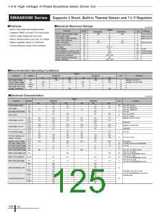
■Electrical Characteristics
(Ta=25°C)
Ratings
SMA6822MP/SLA6827M
Parameter
Symbol
SMA6821MP/SLA6826M
SMA6823MP/SLA6828M
Unit
Conditions
min.
–
typ.
4
max.
min.
–
typ.
4
max.
min.
typ.
4
max.
6
Control Supply Current
Input Voltage
Icc
6
2.5
–
6
–
–
mA
V
Vcc=15V
V
IH
IL
Ihys
IH
IL
UVHL
UVHH
UVhys
–
2
–
2
2.5
–
2
2.5
–
Vcc=15V, Output:ON
Vcc=15V, Output:OFF
Vcc=15V
V
1
1.5
0.5
50
1
1.5
0.5
50
1
1.5
0.5
50
Input Voltage Hysteresis Width
Input Current
V
–
–
–
–
–
–
V
I
–
100
2
–
100
2
–
100
2
Vcc=15V, VIN=5V
Vcc=15V, VIN=0V
µA
I
–
–
–
–
–
–
V
9.0
9.5
–
10.0
10.5
0.5
11.0
11.5
0.5
–
11.0
11.5
–
9.0
9.5
–
10.0
10.5
0.5
11.0
11.5
0.5
–
11.0
11.5
–
9.0
9.5
–
10.0
10.5
0.5
11.0
11.5
0.5
–
11.0
11.5
–
Between VB and U (V, W)
Undevoltage Lock Out
(high side)
V
V
V
V
V
UVLL
10.0
10.5
–
12.0
12.5
–
10.0
10.5
–
12.0
12.5
–
10.0
10.5
–
12.0
12.5
–
Between VCC and COM
Undevoltage Lock Out
(low side)
VUVLH
V
UVhys
V
FOL
0
1.0
5.5
165
135
8.25
1.3
–
0
1.0
5.5
165
135
8.25
1.3
–
0
1.0
5.5
165
135
8.25
1.3
–
V
Vcc=15V
Vcc=15V
FO Pin Output Voltage
V
FOH
4.0
135
105
6.75
–
–
4.0
135
105
6.75
–
–
4.0
135
105
6.75
–
–
Overheat detection threshold
Overheat detection release threshold
Regulator output voltage
TDH
150
120
7.5
1.1
22
150
120
7.5
1.1
22
150
120
7.5
1.1
22
°C
TDL
V
REG
V
V
I
I
REG=35mA
F=0.15A
Boot Diode Forward Voltage
Boot Diode Series Resistance
MOSFET Output Withstand Voltage
MOSFET Output Leakage Current
V
FBD
BD
DSS
DSS
R
–
–
–
Ω
V
V
250
–
–
–
500
–
–
–
500
–
–
–
Vcc=15V, ID=100µA, VIN=0V
I
–
100
–
100
–
100
µA
Vcc=15V, VDS=500V (250V for SMA6821MP/SLA6826M),
Vcc=15V, I
1.25A for SMA6823MP/SLA6828M), VIN=5V
Vcc=15V, I =1.0A (0.75A for SMA6822MP/SLA6827M,
V
IN=0V
D
=1.0A (0.75A for SMA6822MP/SLA6827M,
MOSFET DC On Resistance
Diode Forward Voltage
R
DS(ON)
–
–
1.4
1.0
1.8
1.5
–
–
3.6
1.0
4.0
1.5
–
–
2.0
1.0
2.4
1.5
Ω
D
V
SD
V
1.25A for SMA6823MP/SLA6828M), VIN=0V
td(on)
tr
–
–
–
–
–
–
–
–
–
–
450
100
90
–
–
–
–
–
–
–
–
–
–
–
–
–
–
–
–
–
–
–
–
550
100
120
420
30
–
–
–
–
–
–
–
–
–
–
–
–
–
–
–
–
–
–
–
–
640
100
150
520
30
–
–
–
–
–
–
–
–
–
–
High Side Switching Time
Low Side Switching Time
trr
ns
ns
VBB=300V (150V for SMA6821M/SLA6826M),
td(off)
tf
350
20
Vcc=15V, ID=2A (1.5A for SMA6822M/
SLA6827M, 2.5A for SMA6823M/SLA6828M),
0V≤VIN≤5V
td(on)
tr
550
110
90
570
100
120
450
30
650
100
150
580
30
Inductive load
trr
td(off)
tf
360
20
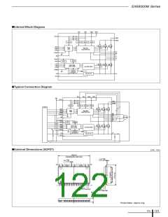
ICs
122

 ETC [ ETC ]