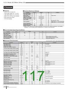
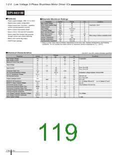
SPI-6631M
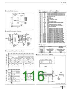
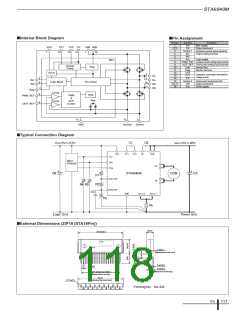
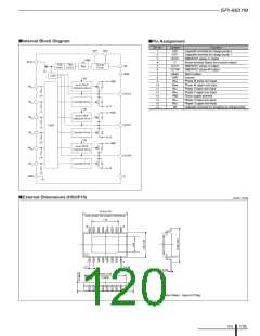
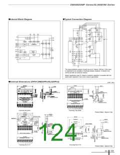
■Internal Block Diagram
■Pin Assignment
Pin No.
Symbol
CP2
CP1
OUTU
S
Function
1
2
Capacitor terminal for charge pump 2
Capacitor terminal for charge pump 1
DMOSFET phase U output
Sense terminal (lower arm source output)
DMOSFET phase V output
DMOSFET phase W output
Alarm output
3
4
5
OUTV
OUTW
Alarm
GND
INLW
6
7
8
Ground
9
Phase W lower arm input
Phase W upper arm input
Phase V lower arm input
Phase V upper arm input
Driver supply terminal
Phase U lower arm input
Phase U upper arm input
Capacitor terminal for charging up charge pump
10
11
12
13
14
15
16
INHW
INLV
INHV
VBB
INLU
INHU
VB
■External Dimensions (HSOP16)
(Unit : mm)
12.20 ± 0.20
(Gate remains: Not included in dimensions)
7.70
16
9
1
8
0.4+–00..0155
1.27
0.25+–00..0155
12.00 ± 0.05
(Cavity)
Product Mass : Approx.0.56g
ICs
119

 ETC [ ETC ]