1-2-5 Low Voltage 3-Phase Brushless Motor Driver ICs
SPI-6631M
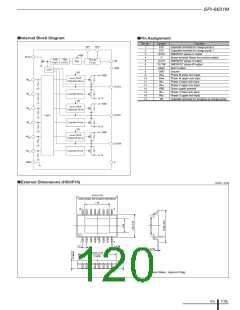
■Features
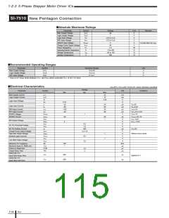
■Absolute Maximum Ratings
• Power supply voltages, VBB: 13 V to 33 V
Parameter
Main Supply Voltage
MOSFET Output Breakdown Voltage
Output Current
Symbol
VBB
Ratings
35
Unit
V
Conditions
DutyCycle=100%*
• Signal power supply configuration
VDSS
Iout
35
V
• Output current Iout: 3 A (max)... repetitive
current (normal-operation current)
±3
A
Input Voltage
VIN
–0.3 to 6.5
–2 to 2
6.5
V
• Built-in current recirculation diode
S Terminal Voltage
Alarm Terminal Voltage
Alarm Input Current
Power Dissipation
Vsen
Valarm
Ialarm
PD
V
• Built-in UVLO, TSD and OCP protection
V
1
mA
W
°C
°C
°C
• Built-in dead time function that prevents
through current upon phase switching
2.67
When using a Sanken evaluation board
Junction Temperature
Storage Temperature
Operating Ambient Temperature
Tj
150
• Built-in error sense flag output
• HSOP16-pin package
Tstg
Ta
–30 to 150
–20 to 85
*: Output current value may be limited, depending on the duty ratio, ambient temperature, and heating
conditions. Do not exceed the rated current or maximum junction temperature (Tj = 150°C).
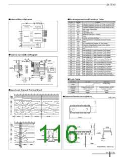
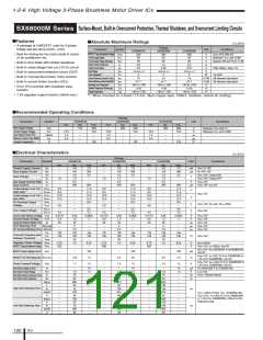
■Electrical Characteristics
(Ta=25°C, VBB=24V, unless otherwise specified)
Ratings
Parameter
Symbol
Unit
Conditions
min.
13
–
typ.
–
max.
33
23
3
Main Supply Voltage
Main Supply Current
Maximum Clock Pulse Width
VBB
IBB
V
mA
µs
V
In operation
–
tw
–
–
VIL
–
–
0.8
–
Input Voltage
Input Current
VIH
IIL
2.0
–
–
V
±8
±20
500
VBB+5
5
–
µA
µA
ns
V
VIN(0), VIN=0.8V
VIN(1), VIN=2.0V
IIH
–
–
Crossover Dead Time
Tdelay
VB
100
–
1200
–
VB Terminal Breakdown Voltage
VB-OUT Breakdown Voltage
VB Terminal Current
Breakdown voltage between VB and GND
VB-OUT
IB
–
–
V
–
–
3
mA
µA
µA
Ω
VB-OUT=5V
VOUT=VBB=35V
VOUT=0V
–
–
800
–
IDSS
Output Leakage Current
–800
–
–
MOSFET ON Resistance
MOSFET Diode Forward Voltage
Overcurrent Sense Current
RDS(ON)
VSD
0.4
–
0.7
2.2
–
IOUT=-1A, Between VBB and OUTꢀꢀIOUT=1A, Between OUT and S
–
V
ISD=1A
IOCP
7
–
A
Short between Out and Out
Overcurrent Protection Blank Time
Overcurrent Protection Delay Time
Thermal Protection Operation Temperature
Thermal Protection Hysteresis
Low Voltage Protection Operation Voltage
Low Voltage Protection Hysteresis
Alarm Output Voltage
tblank
tocp
0.7
0.5
–
1.2
1
4
µs
ms
°C
°C
V
2.2
–
TJ
170
15
4.5
0.45
–
∆TJ
–
–
UVLO
∆UVLO
VAlarm
4.0
0.4
–
5.0
0.5
0.5
VBB voltage
I=1mA
V
V
ICs
118

 ETC [ ETC ]