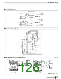
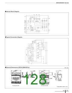
1-2-6 High Voltage 3-Phase Brushless Motor Driver ICs
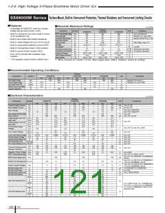
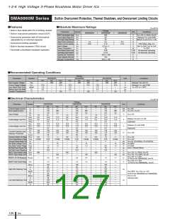
SMA6850M Series Supports 3 Shunt, Built-in Thermal Sensor and 7.5 V Regulator
■Features
■Absolute Maximum Ratings
(Ta=25°C)
Conditions
• Built-in boot diode with limiting resistor
• Supports CMOS (3.3 and 5.0 V) input levels
• Built-in undervoltage lock out circuit
• Built-in thermal sensor (non-stop, Fo output)
• Built-in regulator output (7.5 V/35 mA)
• Current detection using 3 shunt resistors
Ratings
Parameter
Symbol
Unit
SMA6853M
500
SMA6854M
600
MOSFET Output Breakdown Voltage
Control Supply Voltage
V
DSS
CC
BS
V
V
V
CC=15V, I
D=100uA, VIN=0V
V
20
20
Between VCC and COM
Control Supply Voltage (Bootstrap)
Output Current (continuous)
Output Current (pulse)
V
V
Between V
B
and HS (U, V, W)
I
o
2.5
1.5
A
I
op
3.75
2.25
A
PW≦100μs, duty=1%
Regulator Output Current
I
REG
35
–0.5 to +7
28
mA
V
Input Voltage
VIN
Power Dissipation
P
D
W
TC=25C°
Thermal Resistance (Junction to Case)
Thermal Resistance (Junction to Ambient Air)
Operating Case Temperature
Junction Temperature (Power part)
Storage Temperature
θ
θ
T
j-c
j-a
op
4.46
C°W
C°/W
C°
C°
C°
All elements operating
All elements operating
31.25
–20 to +100
150
T
j
Tstg
–40 to +150
■Recommended Operating Conditions
Ratings
Parameter
Symbol
SMA6853M
SMA6854M
Unit
Conditions
min.
–
typ.
300
–
max.
400
16.5
–
min.
–
typ.
300
–
max.
450
16.5
–
Main Supply Voltage
Control Supply Voltage
Minimum Input Pulse Width
Input Signal Dead Time
Junction Temperature
VBB
Vcc
V
V
Between VBB and LS
Between VCC and COM
13.5
0.5
1.5
–
13.5
0.5
1.5
–
Tw(min)
tdead
Tj
–
–
µ
µ
s
s
–
–
–
–
–
125
–
125
°C
■Electrical Characteristics
(Ta=25°C)
Ratings
Parameter
Symbol
SMA6853M
SMA6854M
typ.
Unit
Conditions
min.
–
typ.
4
max.
6
min.
max.
6
Control Supply Current
Input Voltage
I
CC
IH
IL
Ihys
IH
IL
UVHL
UVHH
UVhys
UVLL
UVLH
UVhys
–
–
4
mA
V
V
V
V
V
V
V
CC=15V, IREG=0A
CC=15V, Output:ON
CC=15V, Output:OFF
CC=15V
V
–
2.0
1.5
0.5
50
2.5
2.0
1.5
0.5
50
2.5
–
V
1.0
–
–
–
1.0
–
Input Voltage Hysteresis Width
Input Current
V
–
V
I
–
100
2
–
100
2
CC=15V, VIN=5V
CC=15V, VIN=0V
µA
I
–
–
–
–
V
9.0
9.5
–
10.0
10.5
0.5
11.0
11.5
0.5
–
11.0
11.5
–
9.0
9.5
–
10.0
10.5
0.5
11.0
11.5
0.5
–
11.0
11.5
–
Between V
B and U (V, W)
Undervoltage Lock Out
V
V
V
Hysteresis
V
10.0
10.5
–
12.0
12.5
–
10.0
10.5
–
12.0
12.5
–
Between VCC and COM
Hysteresis
Undervoltage Lock Out
FO Pin Output Voltage
V
V
V
V
V
FOL
FOH
0
1.0
5.5
165
135
–
0
1.0
5.5
165
135
–
V
CC=15V
V
4.0
135
105
–
–
4.0
135
105
–
–
T
DH
150
120
30
150
120
30
Thermal Protection and
Release Threshold
TDL
°C
V
CC=15V, No FIN
T
DHYS
Regulator Output Voltage
Boot Diode Leakage Current
Boot Diode Forward Voltage
Boot Diode Series Resistance
MOSFET Output Breakdown Voltage
V
REG
6.75
–
7.5
–
8.25
10
6.75
–
7.5
–
8.25
10
V
µA
V
I
REG=35mA
ILBD
VR=500V (600V for the SMA6854M)
V
FBD
–
1.1
22
1.3
–
–
1.1
60
1.3
–
IF
=0.15A
R
BD
–
–
Ω
V
V
DSS
500
–
–
600
–
–
V
V
CC=15V, ID=100uA, VIN=0V
CC=15V, VDS=500V
MOSFET Output Leakage Current
MOSFET DC On Resistance
MOSFET Diode Forward Voltage
IDSS
–
–
–
–
100
2.4
1.5
–
–
–
–
100
3.5
1.5
µA
Ω
(600V for the SMA6854M), VIN=0V
CC=15V, I =1.25A
(0.75A for the SMA6854M), VIN=5V
V
D
R
DS (ON)
2.0
1.0
2.8
1.0
V
CC=15V, ISD=1.25A
V
SD
V
(0.75A for the SMA6854M), VIN=0 V
td(on)
tr
–
–
–
–
–
–
–
–
–
–
640
100
150
520
30
–
–
–
–
–
–
–
–
–
–
–
–
–
–
–
–
–
–
–
–
530
55
–
–
–
–
–
–
–
–
–
–
High Side Switching Time
Low Side Switching Time
trr
125
510
50
ns
ns
td(off)
tf
V
BB=300V, VCC=15V, ID=2.5A
(1.5A for the SMA6854M), VIN=0 to 5V
Inductive load
td(on)
tr
650
100
150
580
30
530
60
trr
125
540
55
td(off)
tf
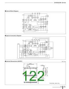
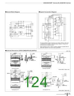
ICs
124

 ETC [ ETC ]