1-2-6 High Voltage 3-Phase Brushless Motor Driver ICs
SX68000M Series Surface-Mount, Built-in Overcurrent Protection, Thermal Shutdown, and Overcurrent Limiting Circuits
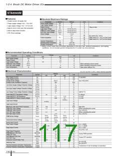
■Features
■Absolute Maximum Ratings
(Ta=25°C)
Conditions
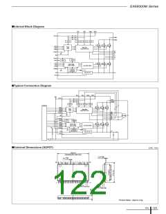
• A package of 6 MOSFET units for 3-phase
bridge and pre-drive (HVIC, LVIC)
Ratings
SX68002M
500
20
20
1.5
2.25
–0.5 to +7
3
15
41.7
–20 to +100
+150
–40 to +150
Parameter
Symbol
Unit
SX68001M
SX68003M
500
• Best for driving the fan motor (built-in motor)
of air conditioner, etc.
MOSFET Output Breakdown Voltage
Control Supply Voltage
VDSS
VCC
VBS
Io
250
20
20
2.0
3.0
V
V
V
A
A
V
W
Vcc=15V,VIN=0V
Between VCC and COM
Between VB and HS (U, V, W)
20
20
2.5
3.75
–0.5 to +7
3
15
41.7
–20 to +100
+150
–40 to +150
Control Supply Voltage (Bootstrap)
Output Current (continuous)
Output Current (pulse)
• Built-in boot diode with limited resistance
• Built-in undervoltage lock out (UVLO) circuit
• Built-in overcurrent protection circuit (OCP)
• Built-in Thermal Shut Down (TSD) function
• Built-in current limiter function (OCL)
Iop
PW≤100µs, duty=1%
Ta=25℃
°C/W All element operation
°C/W All element operation
Input Voltage
Power Dissipation*1
VIN
PD
–0.5 to +7
3
Thermal Resistance (Junction to Case)
Thermal Resistance (Junction toAmbient Air)
Operating Case Temperature
Junction Temperature (Power part)
Storage Temperature
θj-c
θj-a
Top
Tch
Tstg
15
41.7
–20 to +100
+150
–40 to +150
°C
°C
°C
• Error (FO) terminal with shutdown input
function
• 7.5V regulator output function (35mA max.)
*1: When mounted on a board (1.6 mm, 35µm copper layer, CEM-3, moldless, natural air cooling)
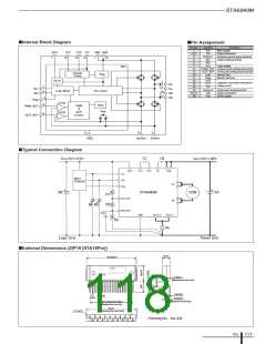
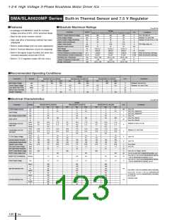
■Recommended Operating Conditions
Ratings
Parameter
Symbol
SX68001M
SX68002M
SX68003M
Unit
Condotions
min.
–
13.5
1.5
0.5
–
typ.
150
–
–
–
max.
200
16.5
–
–
125
min.
–
13.5
1.5
0.5
–
typ.
300
–
–
–
max.
400
16.5
–
–
125
min.
–
13.5
1.5
0.5
–
typ.
300
–
–
–
max.
400
16.5
–
–
125
Main Supply Voltage
VBB
Vcc
tdead
tw
Tj
V
V
µs
µs
°C
Between VBB and LS
Between VCC and COM
Control Supply Voltage
Input Signal Dead Time
Minimum Input Pulse Width
Junction Temperature
–
–
–
■Electrical Characteristics
(Ta=25°C)
Ratings
Parameter
Symbol
SX68001M
SX68002M
SX68003M
Unit
Condotions
min.
–
–
–
1.0
–
typ.
4.6
140
2.0
1.5
0.5
230
–
–
–
–
–
max.
min.
–
–
–
1.0
–
typ.
4.6
140
2.0
1.5
0.5
230
–
–
–
–
–
–
–
–
0.65
1.0
25
max.
min.
–
–
–
1.0
–
typ.
4.6
140
2.0
1.5
0.5
230
–
–
–
–
–
max.
7.4
280
2.5
–
Control Supply Current
Boot Supply Current
Icc
Ibs
7.4
280
2.5
–
7.4
280
2.5
–
mA
µA
Vcc1,2=15V
VB・HS=15V
Vcc=15V, Output:ON
Vcc=15V, Output:OFF
Vcc=15V
VIH
Input Voltage
V
V
IL
Input Voltage Hysteresis Width
Input Current
V
H
–
–
–
V
µA
I
IH
UVHL
UVHH
UVLL
UVLH
–
500
11.0
11.5
12.0
12.5
0.5
–
0.5
5.5
0.6825
1.1
–
–
500
11.0
11.5
12.0
12.5
0.5
–
0.5
5.5
0.6825
1.1
–
–
500
11.0
11.5
12.0
12.5
0.5
–
0.5
5.5
0.6825
1.1
–
Vcc=15V, VIN=5V
V
V
V
V
9.0
9.5
10.0
10.5
–
4.8
–
4.5
0.6175
0.9
20
9.0
9.5
10.0
10.5
–
4.8
–
4.5
0.6175
0.9
20
9.0
9.5
10.0
10.5
–
Undervoltage Lock Out
(high side)
V
V
V
V
Vcc=15V
Undervoltage Lock Out
(low side)
VFOL
FO Terminal Output
Voltage
Vcc=15V, VFO=5V, RFO=10k
Vcc=15V
Ω
V
FOH
–
–
–
4.8
–
–
–
V
OCLL
OCL Output Voltage
V
OCLH
4.5
0.6175
0.9
20
–
–
135
105
–
6.75
500
Current Limiter Reference Voltage
Overcurrent Protection Trip Voltage
Overcurrent Protection Retention Time
OCP Blanking Time
V
LIM
TRIP
tp
0.65
1.0
25
2
3.3
150
120
30
7.5
–
0.65
1.0
25
2
3.3
150
120
30
7.5
–
V
V
µs
µs
µs
Vcc=15V
Vcc=15V
Vcc=15V
Vcc=15V
Vcc=15V
V
tbk(ocp)
–
–
–
–
–
–
2
–
–
–
–
SD Terminal Blanking Time tbk(ocl)
3.3
150
120
30
7.5
–
T
DH
DL
Dhys
135
105
–
6.75
250
165
135
–
8.25
–
135
105
–
6.75
500
165
135
–
8.25
–
165
135
–
8.25
–
Thermal Protection and
Release Threshold
T
T
°C
Vcc=15V
Regulator Output Voltage
V
V
REG
DSS
V
V
I
REG=35mA
Vcc=15V, I
Vcc=15V, VDS=500V(250 V forSX68001M),
IN=0V
Vcc=15V, I
MOSFET Output Breakdown Voltage
D=100µA, VIN=0V
MOSFET Output Leakage Current
MOSFET DC ON Resistance
Diode Forward Voltage
I
DSS
–
–
–
–
100
1.5
1.5
–
–
–
–
100
4.0
1.5
–
–
–
–
100
2.4
1.5
µA
Ω
V
D=1A(0.75 A for SX68002M or
R
DS(ON)
1.25
1.1
3.2
1.0
2.0
1.0
1.25 A for SX68003M), VIN=5V
Vcc=15V, ISD=1A(0.75 A for SX68002M or
1.25 A for SX68003M), VIN=0V
V
SD
V
Boot Diode Leakage Current
Boot Diode Forward Voltage
Boot Diode Reverse Recovery Time
Boot Diode Series Resistance
I
V
trr
R
td(on)
tr
trr
td(off)
tf
td(on)
tr
IB
–
–
–
–
–
–
–
–
–
–
–
–
–
–
–
1.0
70
60
800
45
75
720
40
750
55
70
10
1.3
–
–
–
–
–
–
–
–
–
–
–
–
–
–
–
–
–
–
–
–
–
–
–
–
–
–
1.0
70
60
810
60
120
815
40
760
60
110
750
30
10
1.3
–
–
–
–
–
–
–
–
–
–
–
–
–
–
–
–
–
–
–
–
–
–
–
–
–
–
1.0
70
10
1.3
–
–
–
–
–
–
–
–
–
–
–
µA
V
ns
Ω
VR=500V(250 V for SX68001M)
FB
I
F=0.15A
IF/IRP=100mA/100mA
B
60
940
100
135
975
45
900
105
135
905
35
High Side Switching Time
Low Side Switching Time
ns
ns
VDC=300V(150V for SX68001M),
Vcc=15V, ID=1A(0.75 A for SX68002M
or 1.25 A for SX68003M), HIN=0 to 5V,
Inductive load
trr
td(off)
tf
660
20
–
–
–
ICs
120

 ETC [ ETC ]