SMA6850M Series
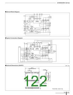
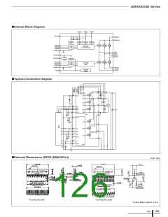
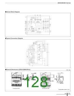
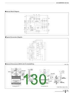
■Internal Block Diagram
VB1(1)
UVLO
VB2(2)
VB3(3)
UVLO
VCC1(4)
VBB1(9)
VBB2(10)
UVLO
UVLO
HIN1(8)
HIN2(7)
HIN3(6)
Input
Logic
High Side
Level Shift Driver
COM1(5)
U(24)
V(12)
VCC2(23)
VREG(16)
W1(11)
W2(14)
7.5V
Reg.
UVLO
LIN1(20)
LIN2(19)
LIN3(18)
Low Side
Driver
Input
Logic
COM2(21)
FO(22)
LS3(15)
LS2(13)
LS1(17)
Thermal
Detect
■Typical Connection Diagram
1
2
3
9
10
VB1 VB2 VB3
4
VCC1
HO1
HS1
24
12
HO2
HS2
M
8
7
6
HIN1
HIN2
HIN3
HO3
HS3
5
11
14
COM1
HVIC
23
VCC2
LO1
LO2
LO3
17
13
15
20
LIN1
LIN2
LIN3
VREG
19
18
16
22
21
FO
COM2
LVIC
15V
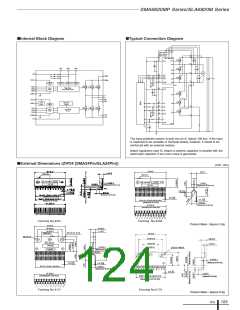
■External Dimensions (ZIP24 [SMA24Pin])
(Unit : mm)
31 0.2
Gate burr
4
0.2
Gate burr
Lot No.
JAPAN
Part No.
Lot No.
JAPAN
1.2 0.1
(Measured at the root)
(Measured at the root)
Part No.
R-end
(Measured at the tip)
+0.15
–0.05
(Measured at the root)
(Measured at the tip)
0.6
+0.15
–0.05
0.5
23 X P1.27 0.5=29.21 0.6
(Measured at the tip)
31.3 0.2
4.5 0.5
(Measured at the tip)
(Including the resin burr)
1
3
5
7
9
11 13 15 17 19 21 23
10 12 14 16 18 20 22 24
2
4
6
8
Forming No.2451
Forming No.2452
Product Mass: Approx. 3.9 g
ICs
125

 ETC [ ETC ]