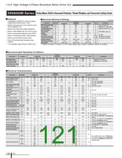
SMA6820MP Series/SLA6820M Series
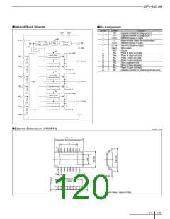
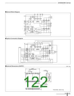
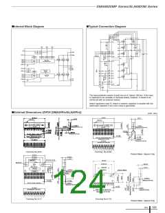
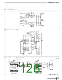
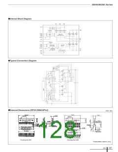
■Internal Block Diagram
■Typical Connection Diagram
1
2
4
11
10
3
5
VB1 VB2 VB3
VCC1
HO1
HS1
24
13
VB1
VB2
VB3
HO2
HS2
M
VD
9
8
7
HIN1
HIN2
HIN3
VBB1
VBB2
HO3
HS3
VCC1
12
14
6
COM3
UVLO
UVLO
UVLO
UVLO
HVIC
HIN1
Input
Logic
High Side
Level Shift Driver
23
HIN2
HIN3
VCC2
COM1
LO1
LO2
LO3
U
V
W1
W2
VCC2
VREG
20
Thermal
Detect
7.5V
Reg.
LIN1
LIN2
LIN3
VREG
UVLO
17
15
19
18
16
LIN1
LIN2
LIN3
Input
Logic
Low Side
Driver
LS2
LS1
COM2
FO
22
21
FO
COM2
LVIC
15V
The input pulldown resistor is built into an IC (about 100 kΩ). If the input
is expected to be unstable or fluctuate widely, however, it needs to be
reinforced with an external resistor.
Attach capacitors near IC. Attach a ceramic capacitor in parallel with the
electrolytic capacitor if too much noise is generated.
■External Dimensions (ZIP24 [SMA24Pin/SLA24Pin])
(Unit : mm)
31 0.2
Gate burr
4
0.2
Gate burr
Lot No.
JAPAN
Lot No.
JAPAN
Part No.
1.2 0.1
(Measured at the root)
Part No.
(Measured at the root)
R-end
(Measured at the tip)
(Measured at the root)
+0.15
–0.05
0.6
+0.15
–0.05
0.5
23 X P1.27 0.5=29.21 0.6
(Measured at the tip)
(Measured at the tip)
4.5 0.5
31.3 0.2
(Measured at the tip)
(Including the resin burr)
1
3
5
7
9
11 13 15 17 19 21 23
10 12 14 16 18 20 22 24
2
4
6
8
Forming No.2451
ꢀꢀForming No.2452
Product Mass : Approx.3.9g
31 0.2
4.8 0.2
1.7 0.1
24.4 0.2
16.4 0.2
Gate burr
φ
3.2 0.15 X 3.8
31 0.2
φ
3.2 0.15
24.4 0.2
4.8 0.2
1.7 0.1
JAPAN
16.4 0.2
Part No.
2.45 0.2
φ3.2 0.15
φ3.2 0.15x3.8
Lot No.
(Measured at the root)
4-(R1)
R-end
2.45 0.1
+0.15
–0.05
+0.15
–0.05
(Measured at the root)
0.6
0.5
23 X P1.27 0.7=29.21
1
4.5 0.7
(Measured at the tip)
+0.2
–0.1
0.6
31.3 0.2
(Including the resin burr)
3
0.3
23xP1.27 0.2=29.21 0.5
(Measured at the tip)
(Measured at the tip)
2
4
6
8
10
12 14
13
16
18
20
22
24
1
3
5
7
9
11
15
17
19
21
23
Forming No.2171
ꢀꢀ Forming No.2175
Product Mass : Approx.6.2g
ICs
123

 ETC [ ETC ]