1-2-4 Brush DC Motor Driver ICs
STA6940M
■Features
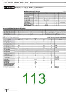
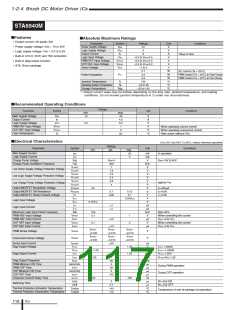
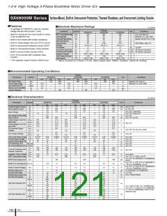
■Absolute Maximum Ratings
• Output current: 4A (peak: 8A)
Parameter
Driver Supply Voltage
Logic Supply Voltage
Output Current
Symbol
VBB
Ratings
Unit
V
Conditions
• Power supply voltage: VBB = 10 to 40V
• Logic supply voltage: VDD = 3.0 to 5.5V
• Built-in UVLO, OCP, and TSD protection
• Built-in diag output function
44
VDD
6
8
V
Io
A
100µs or less
Logic Input Voltage
PWM REF Input Voltage
OCP REF Input Voltage
Sense Voltage
VIN
–0.3 to VDD+0.3
–0.3 to VDD+0.3
–0.3 to VDD+0.3
–1 to 2
V
VPREF
VOREF
VRS
V
V
• STA 18-pin package
V
2.7
W
W
W
°C
°C
°C
DC control (Ta = 25°C)
Power Dissipation
PD
3.0
PWM control (Ta = 25°C) at Slow Decay
PWM control (Ta = 25°C) at Fast Decay
3.2
Junction Temperature
Operating Ambient Temperature
Storage Temperature
Tj
Ta
150
–20 to 85
–30 to 150
Tstg
*: Output current value may be limited, depending on the duty ratio, ambient temperature, and heating
conditions. Do not exceed junction temperature of Tj under any circumstances.
■Recommended Operating Conditions
Ratings
Parameter
Symbol
Unit
Conditions
min.
10
max.
40
4.0
5.5
1
Main Supply Voltage
Output Current
VBB
Io
V
A
Logic Supply Voltage
PWM REF Input Voltage
OCP REF Input Voltage
Case Temperature
VDD
VPREF
VOREF
Tc
3.0
V
V
When operating current control
When operating overcurrent control
Rear center (without Fin)
2
V
85
°C
■Electrical Characteristics
(VDD=5V, VBB=24V, Ta=25°C, unless otherwise specified)
Ratings
typ.
Parameter
Symbol
Unit
Concitions
min.
max.
20
Main Supply Current
Logic Supply Current
Charge Pump Voltage
Charge Pump Oscillation Frequency
IBB
IDD
mA
mA
V
In operation
5
Vcp
VBB+5
360
7
VBB=10V to 40V
Fcp
kHz
V
VUVBL
VUVBH
VUVDL
VUVDH
VUVCL
VUVCH
V(BR)DS
RDS(ON)
VF
Low Driver Supply Voltage Protection Voltage
Low Logic Supply Voltage Protection Voltage
Low Charge Pump Voltage Protection Voltage
7.8
2.3
2.5
3.8
4
V
V
V
V
against VBB
V
Output MOSFET Breakdown Voltage
Output MOSFET ON Resistance
Output MOSFET Diode Forward Voltage
60
V
ID=250µA
ID=4.0A
IF=4.0A
0.1
0.13
2.1
Ω
0.95
V
VLIL
0.25VDD
V
Logic Input Voltage
Logic Input Current
VLIH
0.75VDD
V
ILIL
±1
±1
µA
µA
kHz
V
ILIH
Maximum Logic Input Clock Frequency
PWM REF Input Voltage
PWM REF Input Current
OCP REF Input Voltage
OCP REF Input Current
fclk
100
0.1
duty=50%
VPREF
IPREF
VOREF
IOREF
1
2
When controlling the current
VREF=0 to VDD
When controlling the current
VREF=0 to VDD
±10
µA
V
0.1
±10
VPREF
–0.015
VOREF
–0.015
±20
µA
VPREF
–0.045
VOREF
–0.045
VPREF
+0.015
VOREF
VPSEN
VOSEN
V
V
PWM Sense Voltage
Overcurrent Sense Voltage
+0.015
Sense Input Current
Diag Output Voltage
ISENSE
VLOL
µA
V
1.25
1.25
ILOL=1.25mA
ILOL=–1.25mA
VLOL=1.25V
VLOH
VDD–1.25
–1.25
V
Diag Output Current
ILOL
mA
mA
kHz
µs
ILOH
VLOH=VDD-1.25
Diag Output Frequency
PWM Minimum ON Time
PWM OFF Time
OCP Minimum ON Time
OCP OFF Time
fDIAG
90
5
tpon(min)
tPOFF
During PWM operation
During OCP operation
35
5
µs
toon(min)
tOOFF
µs
142
µs
Crossover Current Delay Time
tCOCD
tcon
150
750
ns
µs
3
IN→Out ON
IN→Out OFF
Switching Time
tcoff
2.7
140
115
µs
Thermal Protection Activation Temperature
Thermal Protection Deactivation Temperature
Ttsdon
Ttsdoff
°C
°C
Temperature of rear of package (at saturation)
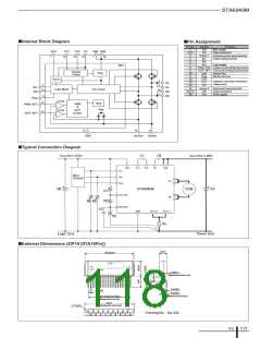
ICs
116

 ETC [ ETC ]