STA6940M
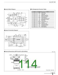
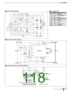
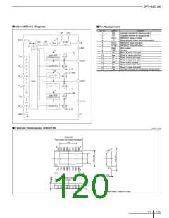
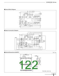
■Internal Block Diagram
■Pin Assignment
Pin No.
Symbol
VBB
OA
Sense 1
IN1
Function
1
2,3
4
Main supply
Output terminal A
Constant current sense terminal
Output setting terminal
VDD
CP1
13
CP2 CP
12 14
VBB VBB
1 18
7
5
6
IN2
7
8
9
VDD
Logic supply
MIC
PWM_REF Constant current setting input terminal
OCP_REF Overcurrent setting input terminal
Charge
Pump
Reg
10
11
12
13
14
15
16,17
18
Gnd
Diag
CP2
CP1
CP
Sense 2
OB
VBB
Device Gnd
Monitor terminal
UVLO
Capacitor connection terminal for
charge pump
2
3
OA
OA
OB
OB
5
6
IN1
IN2
Overcurrent sense terminal
Output terminal B
Driver supply
Logic Block
Pre_Driver
16
17
11
8
Diag
Comp
Comp
OSC
Reg
PWM
&
OCP
PWM_REF
9
OCP_REF
Control
10
GND
15
4
Sense2
Sense1
■Typical Connection Diagram
■External Dimensions (ZIP18 [STA18Pin])
4±0.2
25.25±0.3
Lot No
Type No
1.3±0.1
(Measured at the root)
R-end
+0.2
0.45
–0.1
+0.2
0.55
–0.1
2.54±0.5
(Measured at the tip)
17xP1.27±0.5=21.59±1
(Measured at the tip)
25.55
C1.5±0.5
(Including the resin burr)
Forming No. No.434
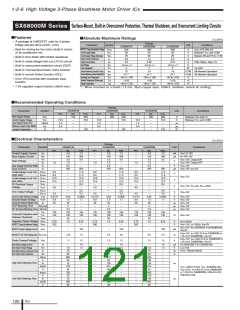
ICs
117

 ETC [ ETC ]