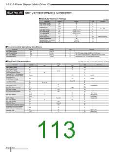
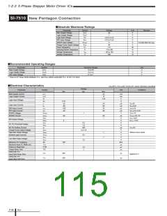
SLA7611M
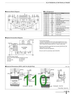
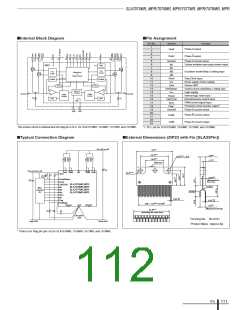
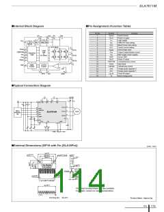
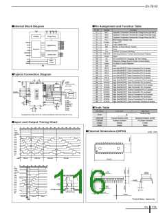
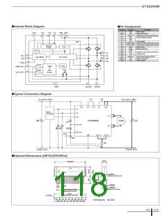
■Internal Block Diagram
■Pin Assignment (Function Table)
Pin No.
1
Symbol
Sense
Out U
Function
Current sense
Phase U output
Logic supply
VB
18
VBB
9
CP1
16
CP2
2
15
3
VCC
VCC
3
TSD
Reg
Charge Pump
PWM OFF time setting
Mixed Decay ratio setting
Control current setting
Internal logic reset
4
RC
PFD
REF
Reset
Ena
UVLO
5
OUT Block
2
6
13
12
14
8
Clock
7
OUT
U
V
Level
shift
&
CW/CCW
F/H
Output Enable/Disable control
Main supply (motor supply)
Device GND
8
11
Sequence
Logic
9
VBB
OUT
Pri-Driver
10
11
12
13
14
15
16
17
18
GND
Out V
Ena
17
1
Phase V output
Reset
7
OUT
S
W
Forward/reverse control
Step Clock
CW/CCW
Clock
+
_
Current
Control
REF
6
PWM
Full/half step control
Charge pump capacitor 2
Charge pump capacitor 1
Phase W output
Full/Half
CP2
Control
CP1
5
4
10
Out W
PFD
RC
GND
Boost charge pump
V
B
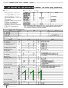
■Typical Connection Diagram
C2
C1
10 to 30V
+
16
15
CP2
18
VB
9
5V
CA
C5
3
VCC CP1
VBB
CB
C4 C3
+
2
OUTU
OUTV
13
12
14
8
Clock
CW/CCW
F/H
11
Micro-
computer,
etc.
φ
3
SPM
SLA7611M
Ena
17
1
OUTW
S
7
Reset
R2
R4
6
REF
PFD
RC
GND
5
4
10
Rs
Ct
Rt
R1
R5
R3
S-GND
P-GND
■External Dimensions (ZIP18 with Fin [SLA18Pin])
(Unit : mm)
31±0.2
24.4±0.2
16.4±0.2
φ3.2±0.15
φ3.2±0.15×3.8 4.8±0.2
1.7±0.1
Part Number
Lot number
2.45±0.2
R-End
+0.2
–0.1
+0.2
+0.2
0.65
1
–0.1
0.55
4±0.7
–0.1
17×P1.68±0.4=28.56±1
31.3±0.2
Other lead forming shapes are also available.
For details, contact our sales representative.
.
. . . . . . .
18
1 2 3
Forming No. No.871
Product Mass : Approx.6g
ICs
113

 ETC [ ETC ]