1-2-2 3-Phase Stepper Motor Driver ICs
SLA7611M Star Connection/Delta Connection
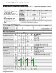
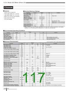
■Absolute Maximum Ratings
(Ta=25°C)
Remarks
Parameter
Main Supply Voltage
Logic Supply Voltage
Symbol
Ratings
Unit
V
VBB
36
V
CC
7
V
I
O (Ave)
O (Peak)
IN
3
6
A
Output Current
I
A
tw < 1ms
Logic Input Voltage
REF Input Voltage
PFD Input Voltage
Sense Voltage
V
–0.3 to VCC+0.3
–0.3 to VCC+0.3
–0.3 to VCC+0.3
–2 to 2
V
V
V
REF
PFD
V
V
VRs
V
Power Dissipation
P
D
4
W
°C
°C
°C
Without heatsink
Junction Temperature
Operating Ambient Temperature
Storage Temperature
T
j
150
Ta
–20 to 85
–30 to 150
Tstg
■Recommended Operating Conditions
Parameter
Symbol
Ratings
Unit
Remarks
Main Supply Voltage
Logic Supply Voltage
REF Input Voltage
Case Temperature
V
V
V
BB
10 to 30
3 to 5.5
V
V
CC
The VCC surge voltage should be 0.5V or lower.
The control current precision is degraded at 0.2V or lower.
Temperature at Pin-10 Lead (without heatsink)
REF
0.2 to VCC
110max
V
T
C
°C
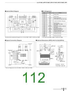
■Electrical Characteristics
(Ta=25°C, VBB=24V, VCC=5V, unless otherwise specified)
Ratings
typ.
Parameter
Symbol
Unit
Remarks
min.
36
max.
20
Main Supply Current
I
I
BB
cc
mA
mA
V
10
Logic Supply Current
Charge Pump Voltage
Output Breakdown Voltage
VB
VBB+5
VO
V
Output MOS FET ON Resistance
(total of the upper and lower values)
0.8
1.5
R
DS (on)
Ω
I
I
DS=3A
SD=3A
Output MOS FET
Diode Forward Voltage
VSD
V
V
CC×0.25
V
IL
V
V
Logic Input Voltage
Logic Input Current
VIH
V
CC×0.75
I
I
IL
IH
clock
PFD
RC
±1
±1
µA
µA
kHz
µA
µA
V
Excluding Ena
100
Maximum Clock Frequency
PFD Input Current
F
I
±10
RC Terminal Inflow Current
I
200
VCC
V
V
V
V
V
PFDS
PFDM
PFDF
Rs
1.7
0.7
Slow Decay
Mixed Decay
Fast Decay
Steady-state
1.3
0.3
PFD Input Voltage
V
V
Sense Voltage
V
REF×0.2
V
VCC
REF Input Voltage
REF
0
V
REF Input Current
I
REF
±10
µA
µs
°C
PWM OFF Time
T
T
OFF
j
1.1×Rt×Ct
Thermal Protection Circuit Activation Temperature
150
Hysteresis of Thermal Protection
Circuit Activation Temperature
∆Tj
10
°C
T
ONC
2.5
2
µs
µs
Clock→Out
Clock→Out
Switching Time
T
OFFC
ICs
112

 ETC [ ETC ]