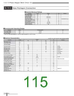
1-2-3 5-Phase Stepper Motor Driver ICs
SI-7510 New Pentagon Connection
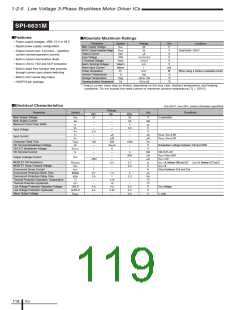
■Absolute Maximum Ratings
Parameter
Symbol
Ratings
Unit
V
Remarks
Main Supply Voltage
Logic Supply Voltage
Logic Input Voltage
V
CC
1
2
44
VCC
7
–0.3 to VCC
–0.3 to VCC
2
V
V
IN
REF
SENCE
MC3
2
2
V
REF Input Voltage
V
V
SENCE Input Voltage
Charge Pump Output Voltage
Power Dissipation
V
V
Except when tw<1µs
V
48
V
P
D
1.6
W
°C
°C
°C
Operating Ambient Temperature
Storage Temperature
Junction Temperature
Ta
–10 to 80
Tstg
–20 to 150
150
Tj
■Recommended Operating Ranges
Parameter
Main Supply Voltage
Logic Supply Voltage
REF Input Voltage
Symbol
Operating Ranges
10 to 42*
Unit
V
VCC1
VCC2
3 to 5.5
V
VREF
0.1 to 1
V
*: Insert a 5V Zener diode between VCC1 and VMC3 when using with VCC1 of 35 V or more.
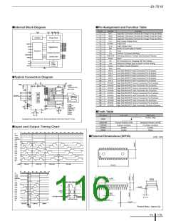
■Electrical Characteristics
(Ta=25°C, Vcc1=24V, VCC2=5V, unless otherwise specified)
Ratings
typ.
Parameter
Symbol
Unit
Conditions
min.
max.
25
Main Supply Current
Logic Supply Current
I
CC
1
2
mA
mA
V
ICC
10
V
IL
1.25
Logic Input Voltage
Logic Input Current
V
IH
3.75
–20
V
I
IL
IH
ENA
REF
SENCE
SENCE
20
20
20
20
µA
µA
µA
µA
V
V
V
V
V
V
V
IL=0V
I
–20
IH=5.5V
ENA=0V
ENA Input Current
REF Input Current
SENCE Voltage
SENCE Current
I
–100
–20
I
REF=0 to 5.5V
REF=1V
V
1
I
–20
4
20
1
µA
V
SENCE=0V, 2V
V
V
V
V
MOL
MOH
RCL
RCH
I
I
MOL=1mA
MO Output Voltage
V
MOH=–1mA
0.5
1.5
300
V
RC Pin Threshold Voltage
V
RC Pin Outflow Current
Charge Pump Output Voltage
High Side Output Voltage
(between gate sources)
I
RC
µA
V
VRC=0V
V
V
V
V
V
MC3
VCC1+9
Without Zener diode
HGSL
HGSH
LGL
1
1
V
8.5
V
V
Low Side Output Voltage
LGH
7.5
V
Maximum CL Frequency
Maximum Input CL Width (on)
Power-on Reset time
Output Delay Time
fck
100
1
KHz
µs
µs
µs
TCON
PTW
TIO
1.5
2
CW/CCW, F/H
T
ICS
500
500
µs
µs
Against CL ↑
Input Data Setup Time
CW/CCW, F/H
TICH
Input Data Hold Time
ICs
114

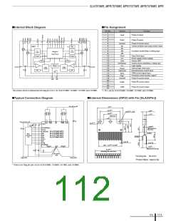
 ETC [ ETC ]