SLA7075MR, MPR/7076MR, MPR/7077MR, MPR/7078MR, MPR
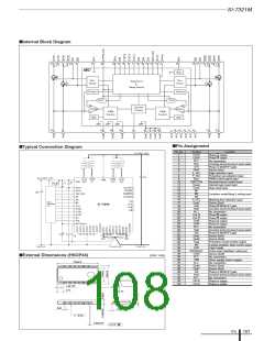
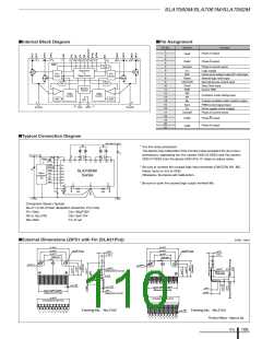
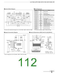
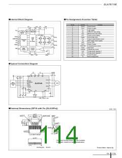
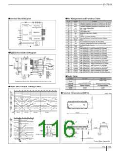
■Internal Block Diagram
■Pin Assignment
Pin No.
Symbol
Function
1
2
3
4
OutA
Phase A output
Phase A output
OutA/
8
9
16 10 15
11
20 21 22 23
1
2
3
4
14
15
18
6
7
5
SenseA
Phase A current sense
6
7
8
9
M
O
2 phase excitation state output monitor output
Reg
MIC
M1
M2
Pre-
Driver
Pre-
Driver
Excitation mode/Sleep 2 setting input
Sequencer
&
Sleep Circuit
M3
10
11
12
13
14
15
16
17
18
19
20
21
22
23
Clock
Step Clock input
Protect
Protect
VBB
Driver supply (motor supply)
Device GND
Gnd
DAC
DAC
Control current mode/Sleep 1 setting input
Logic supply
Ref/Sleep1
+
–
+
Synchro
Control
V
DD
19
–
5
SenseA
SenseB
PWM
Control
PWM
Control
Internal logic reset input
Normal/reverse control input
PWM control signal input
Protection circuit monitor output*1
Phase B current sense
Reset
CW/CCW
Sync
R
S
OSC
RS
OSC
Flag*1
17
Sync
12
Gnd
SenseB
Phase B current output
Phase B current output
OutB/
OutB
The protect circuit is deleted and the flag pin is N.C. for SLA7075MR, 7076MR, 7077MR, and 7078MR.
*1: N.C. pin for SLA7075MR, 7076MR, 7077MR, and 7078MR.
■Typical Connection Diagram
■External Dimensions (ZIP23 with Fin [SLA23Pin])
Vs=10V to 44V
31±0.2
24.4±0.2
16.4±0.2
4.8±0.2
1.7±0.1
3.2±0.15 × 3.8
φ
Gate burr
+
CA
Vcc=3.0V to 5.5V
OutA OutA
±0.15
BB
OutB OutB
φ
3.2
VDD
C1
r1
Q1
2.45±0.2
(Measured at
the root)
Reset/Sleep1
Clock
CB
SLA7075MR,MPR
SLA7076MR,MPR
SLA7077MR,MPR
SLA7078MR,MPR
CW/CCW
M1
4–(R1)
Micro-
computer,
etc.
M2
R-end
M3
Sync
MO
+0.2
–0.1
0.65
+0.2
Flag
0.55
–0.1
Ref/Sleep
22P × 1.27±0.5=27.94±1
SenseA
Gnd
SenseB
4.5±0.7
(Measured at the tip)
31.3±0.2
r2
r3
C2
(Including the resin burr)
One-point
Gnd
Forming No. No.2151
Logic Gnd
Power Gnd
Product Mass : Approx.6g
* There is no Flag pin (pin 18) for SLA7075MR, 7076MR, 7077MR, and 7078MR.
ICs
111

 ETC [ ETC ]