SLA7060M/SLA7061M/SLA7062M
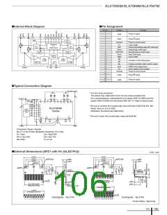
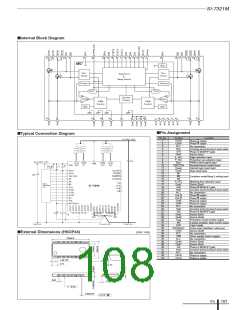
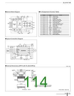
■Internal Block Diagram
■Pin Assignment
Pin No.
Symbol
Function
1
Phase A output
Phase A output
OutA
2
3
1
2
3
4
7
6
14 13 12
9
10
8
16
Reg
18
19 20
21
OutA/
4
MIC
5
SenseA
Phase A current sense
Logic supply
Sequencer
&
Sleep Circuit
6
VDD
Pre-
Driver
Pre-
Driver
7
REF
Reset
CW/CCW
Clock
GND
Control current setting & output OFF control input
Internal logic reset input
Normal/reverse control input
Step Clock input
8
9
DAC
DAC
10
11
12
13
14
15
16
17
18
19
20
21
Synchro
Control
–
+
–
Device GND
+
M2
PWM
Control
PWM
Control
Excitation mode setting input
M1
OSC
OSC
M
O
2-phase excitation state monitor output
PWM control signal input
5
17
SenseB
Sync
15
11
GND
SenseA
Sync
V
BB
Driver supply (motor supply)
Phase B current sense
SenseB
OutB/
Phase B output
Phase B output
OutB
■Typical Connection Diagram
VBB=VM=10~44V
* VDD line noise precaution:
The device may malfunction if the VDD line noise exceeds 0.5V. As a coun-
termeasure, separating the VDD system GND (S-GND) and VBB system
GND (P-GND) from the device GND (Pin-11) helps to reduce noise.
CA
V
DD=3.0~5.5V
R1
C1
Disable
Q1
6
16
1
2
3
4
18 19
20 21
Reset
8
CW/CCW
Clock
M2
* Be sure to connect the unused logic input terminals (CW/CCW, M1, M2,
Reset, Sync) to VDD or GND.
9
CB
10
12
13
14
15
SLA7060M
Series
Micro-
computer,
etc.
Otherwise, the device will malfunction.
M1
M
O
Sync
* Be sure to open the unused logic output terminal Mo.
5
11
17
7
R2
R3
RsA
RsB
S-GND
P-GND
Component Values (Typical)
.
2×Rs)
=
Rs=0.1 to 2Ω (Power dissipation should be: P I
O
.
R1=10kΩ
CA=100µF/50V
CB=10µF/10V
C1=0.1µF
R2=5.1kΩ (VR)
R3=10kΩ
■External Dimensions (ZIP21 with Fin [SLA21Pin])
(Unit : mm)
±0.2
±0.2
31.0
31.0
±0.2
±0.2
±0.15
±0.2
±0.2
±0.15
φ 3.2 ×3.8
24.4
16.4
φ
3.2
×3.8
24.4
16.4
±0.2
±0.1
±0.2
±0.1
4.8
1.7
4.8
1.7
Gate burr
Gate burr
±0.15
3.2
φ
±0.15
φ 3.2
±0.2
2.45
[Measured at the root]
±0.2
2.45
[Measured
at the root]
4–[R1]
R-end
+0.2
–0.1
0.65
+0.2
–0.1
±0.5
±0.7
0.55
20×P1.43
=28.6
±0.6
±0.6
6
[Measured at the tip]
±0.5
±1
=28.6
±0.7
20×P1.43
4
7.5
[Measured at the tip]
[Measured at the tip]
±0.2
31.3
±0.2
31.3
[Including the resin burr]
[Including the resin burr]
+0.2
–0.1
1
3
5
7
9
11 13 15 17 19 21
10 12 14 16 18 20
Forming No. No.2102
Forming No. No.2104
0.65
2
4
6
8
1
3
5
7
9
11 13 15 17 19 21
10 12 14 16 18 20
2
4
6
8
Product Mass : Approx.6g
ICs
109

 ETC [ ETC ]