DM9101
10/100Mbps Ethernet Physical Layer Single Chip Transceiver
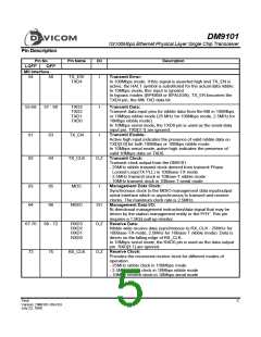
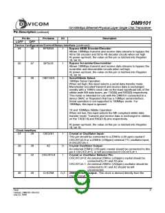
Pin Description
Pin No.
Pin Name
I/O
Description
LQFP
QFP
MII Interface
Transmit Error:
54
56
TX_ER/
TXD4
I
In 100Mbps mode, if this signal is asserted high and TX_EN is
active, the HALT symbol is substituted for the actual data nibble.
In 10Mbps mode, this input is ignored.
In bypass modes (BP4B5B or BPALIGN), TX_ER becomes the
TXD4 pin, the fifth TXD data bit.
Transmit Data:
55-58
57 - 60
TXD3
TXD2
TXD1
TXD0
I
Transmit data input pins for nibble data from the MII in 100Mbps
or 10Mbps nibble mode (25 MHz for 100Mbps mode, 2.5MHz for
10Mbps nibble mode).
In 10Mbps serial mode, the TXD0 pin is used as the serial data
input pin. TXD[3:1] are ignored.
Transmit Enable:
61
62
63
64
TX_EN
I
Active high input indicates the presence of valid nibble data on
TXD[3:0] for both 100Mbps or 10Mbps nibble mode.
In 10Mbps serial mode, active high indicates the presence of
valid 10Mbps data on TXD0.
Transmit Clock:
TX_CLK
O,Z
Transmit clock output from the DM9101:
- 25MHz nibble transmit clock derived from transmit Phase
Locked Loop(TX PLL) in 100Base-TX mode
- 2.5MHz transmit clock in 10Base-T nibble mode
- 10MHz transmit clock in 10Base-T serial mode
Management Data Clock:
Synchronous clock to the MDIO management data input/output
serial interface which is asynchronous to transmit and receive
clocks. The maximum clock rate is 2.5MHz.
Management Data I/O:
63
64
65
66
MDC
I
MDIO
I/O
O,Z
Bi-directional management instruction/data signal that may be
driven by the station management entity or the PHY. This pin
requires a 1.5KΩ pull-up resistor.
Receive Data:
67-70
69 - 72
RXD3
RXD2
RXD1
RXD0
Nibble wide receive data (synchronous to RX_CLK - 25MHz for
100Base-TX mode, 2.5MHz for 10Base-T nibble mode). Data is
driven on the falling edge of RX_CLK.
In 10Mbps serial mode, the RXD0 pin is used as the data output
pin. RXD[3:1] are ignored.
Receive Clock:
73
75
RX_CLK
O,Z
Provides the recovered receive clock for different modes of
operation:
- 25MHz nibble clock in 100Mbps mode
- 2.5MHz nibble clock in 10Mbps nibble mode
- 10MHz receive clock in 10Mbps serial mode
Final
5
Version: DM9101-DS-F03
July 22, 1999

 ETC [ ETC ]