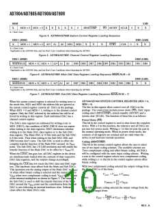
AD7804/AD7805/AD7808/AD7809
AD7805/AD7809 PIN FUNCTION DESCRIPTIONS
AD7805 AD7809
Pin No. Pin No.
Mnemonic
Description
1, 11, 13,
20, 33
NC
No Connect. These pins should be left open circuit.
1
2, 3
4
5–10,
12, 13
19, 20
2, 5, 39, 40
41, 42
43
3, 4, 6, 7, 9, DB9–DB2
10, 15, 23
AGND
Ground reference point for analog circuitry.
Analog output voltages from the DACs.
Reference Output. This is a bandgap reference and is typically 1.23 V.
Data Inputs. DB9 to DB2 are the 8 MSBs of the data word.
V
OUTB, VOUT
A
E
REFOUT
24, 26
DB1, DB0
DB1 and DB0 function as the 2 LSBs of the 10-bit word in 10-bit parallel mode but
have other functions when BYTE loading structure is used.
Analog output voltages from the DACs.
LDAC Input. When this digital input is taken low, all DAC registers are simultaneously
updated with the contents of the DAC data registers. If LDAC is permanently tied low, or is
low during the rising edge of WR similar to data inputs, an automatic update will take place.
Ground reference point for digital circuitry.
Digital Power Supply.
Write Input WR is an active low logic input which is used in conjunction with CS and
the address pins to write data to the relevant registers.
8, 12
14
VOUTF, VOUT
LDAC
11
14
15
16
16
17
18
DGND
DVDD
WR
17
18
21
19
CS
CLR
Chip Select. Active low logic input.
Asynchronous CLR Input. When this input is taken low, all Main DAC outputs are
cleared either to VBIAS or to VBIAS/16 volts. All Sub DACs are also cleared and thus the
transfer function of the MAIN DAC will remain centered around the VBIAS point.
Analog output voltages from the DACs.
22, 25
VOUTH, VOUTG
21, 22
27, 29, 30
A2, A1, A0
DAC Address Inputs. These digital inputs are used in conjunction with CS and WR to
determine which DAC channel control register or DAC data register is loaded from the
input register. These address bits are don’t cares when writing to the system control register.
Logic Input. Logic high enables writing to the DAC data registers, a logic low enables
writing to the control registers.
This is an external reference input for the DAC. When this reference is selected for the DAC
in the control register, the analog output from the selected DAC swings around this point.
Compensation Pin. This pin provides an output from the internal VDD/2 divider and is
provided for ac bypass purposes only. This pin should be decoupled with 1 nF capacitors
to both AVDD and AGND. This pin can be overdriven with an external reference, thus
giving the facility for two external references on the part.
23
24
25
31
32
34
MODE
REFIN
COMP
26, 27
28
35, 36
28, 37, 38
44
VOUTD, VOUT
AVDD
PD
C
Analog output voltages from the DACs.
Analog Power Supply.
Active low input used to put the part into low power mode reducing current consump-
tion to 1 µA.
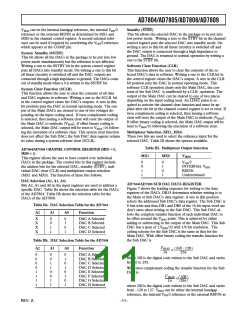
AD7805 PIN CONFIGURATION
AD7809 PIN CONFIGURATION
1
2
3
4
5
6
7
8
9
28
27
26
25
AGND
AV
V
DD
V
B
A
C
OUT
OUT
44 43 42 41 40 39 38 37 36 35 34
V
V
D
OUT
OUT
REFOUT
DB9
COMP
1
33
32
31
30
29
28
27
26
25
24
23
NC
NC
PIN 1
IDENTIFIER
2
3
REFIN
MODE
A0
AGND
DB9
24 REFIN
DB8
23
22
21
MODE
A0
AD7805
TOP VIEW
(Not to Scale)
4
DB8
DB7
5
AGND
DB7
A1
AD7809
TOP VIEW
(Not to Scale)
DB6
A1
6
AV
DD
DB5
20 DB0
7
A2
DB6
8
DB0
V
F
DB4 10
11
19
18
17
16
15
DB1
OUT
9
V
G
DB5
DB4
NC
OUT
LDAC
CLR
CS
10
11
DB1
DB2
12
13
14
DB3
DB2
WR
DV
12 13 14 15 16 17 18 19 20 21 22
DGND
DD
NC = NO CONNECT
–8–
REV. A

 ETC [ ETC ]