AD7804/AD7805/AD7808/AD7809
determined by MX1 and MX0 in the channel control register as
shown in Table III. The internal VDD/2 reference is provided at
the COMP pin. This internal reference can be overdriven with
an external reference thus providing the facility for two external
references.
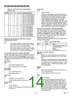
POWER-UP
WRITE TO SYSTEM
CONTROL REGISTER
SYSTEM
CONFIGURATION
WRITE TO CHANNEL
CONTROL REGISTER
CHANNEL
CONFIGURATION
AD7804/AD7808 POWER-UP CONDITIONS
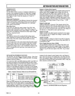
When power is applied to the device, the device will come up in
standby mode where all the linear circuitry excluding the refer-
ence are switched off. Figure 8 shows the relevant default val-
ues for the system control register. Since a write to the system
control register is required to remove the standby condition the
only bits for which default conditions are applicable are PD and
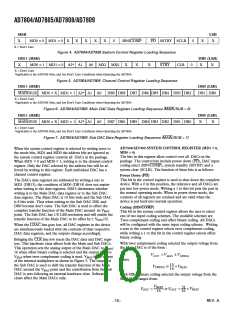
SSTBY. Figure 9 details the relevant default conditions for the
Channel Control Register.
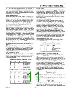
N
ALL CHANNELS
CONFIGURED
Y
WRITE TO SELECTED
MAIN OR SUB DAC
DATA REGISTERS
DATA WRITE
N
DATA LOADING
COMPLETE
PD
SSTBY
1
1
Y
CHANGE
CHANNEL
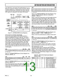
Figure 8. Default Conditions for System Control Register
on Power-Up
Y
Y
CONFIGURATION
N
STBY
CLR
MX1
MX0
CHANGE
SYSTEM
CONFIGURATION
1
1
0
0
Figure 9. Default Conditions for Channel Control Register
on Power-Up
N
END
After power has been applied to the device the following proce-
dure should be followed to communicate and set up the device.
First, a write to the system control register is required to clear
the SSTBY bit and change the input coding scheme if required.
Figure 10. Flowchart for Controlling the DAC Following
Power-Up
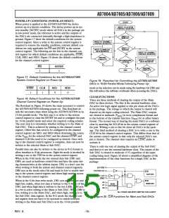
AD7805/AD7809 INTERFACE SECTION
For example, to remove standby and set up offset binary input
coding 0060Hex should be written to the input register, if twos
complement coding is required 0020Hex should be written to
the input register. MD1 and MD0 are decoded in the input
register and this allows the data to be written to the system
control register.
The AD7805 and AD7809 are parallel data input devices and
contain both control registers and data registers. The system
control register has global control over all DACs in the package
while the channel control register allows control over individual
DACs in the package. Two data registers are also available, one
for the 10-bit Main DAC and the second for the 8-bit Sub
DAC. In the parallel mode, CS and WR, in association with the
address pins, control the loading of data. Data is transferred
from the data register to the DAC register under the control of
the LDAC signal. Only data contained in the DAC register deter-
mines the analog output of any DAC. The timing diagram for
10-bit parallel loading is shown in Figure 2. The MODE pin on
the device determines whether writing is to the data registers or
to the control registers. When MODE is at a logic one, writing
is to the data registers. In the next write to the data registers a
bit in the channel control register determines whether the Main
DAC or the Sub DAC is addressed. This means that to address
either the Main or the Sub DAC the Main/Sub bit in the control
register has to be set appropriately before the data register write.
A logic zero on the mode pin enables writing to the control
register. Bit MD0 determines whether writing is to the system
control register or to the addressed channel control register.
Step two requires writing to the channel control register, which
allows individual control over each DAC in the package and
allows the VBIAS for the DAC to be selected as well as individual
DAC standby and clear functions. For example, if channel A is
to be configured for normal operation with internal reference
selected then 4110Hex should be written to the input register.
In the input register, the MD1 and MD0 bits are decoded in
association with the address bits to give access to the required
channel control register. The third and final step is to write data
to the selected DAC. To write half scale to channel A Main
DAC, 2200Hex should be written to the input register, the
MSB in the sixteen bit stream selects the Main DAC and the
next three bits address the DAC and the final 10 bits contain
the data. To write half scale to channel A Sub DAC, then A200
should be written to the input register. The flowchart in Figure
10 shows in graphic form the steps required in communicating
with the AD7804/AD7808.
Bringing the CLR line low resets the DAC registers to one of
two known conditions depending on the coding scheme se-
lected. The hardware clear affects both the Main and Sub
DAC registers. With offset binary coding a clear sets the output
–12–
REV. A

 ETC [ ETC ]