AD7804/AD7805/AD7808/AD7809
TERMINOLOGY
Relative Accuracy
Digital-to-Analog Glitch Impulse
Digital-to-analog glitch impulse is the impulse injected into the
analog output when the digital inputs change state with the
DAC selected and the LDAC used to update the DAC. It is
normally specified as the area of the glitch in nV-s and is mea-
sured when the digital input code is changed by 1 LSB at the
major carry transition. Regardless of whether offset binary or twos
complement coding is used, the major carry transition occurs at
the analog output voltage change of VBIAS to VBIAS – 1 LSB
or vice versa.
For the DACs, relative accuracy or endpoint nonlinearity is a
measure of the maximum deviation, in LSBs, from a straight
line passing through the endpoints of the DAC transfer func-
tion. Figures 32 and 33 show the linearity at 3 V and 5 V
respectively.
Differential Nonlinearity
Differential nonlinearity is the difference between the measured
change and the ideal 1 LSB change between any two adjacent
codes. A specified differential nonlinearity of ±1 LSB maxi-
mum ensures monotonicity.
Digital Feedthrough
Digital feedthrough is a measure of the impulse injected into
the analog output of a DAC from the digital inputs of the same
DAC but is measured when the DAC is not updated. It is speci-
fied in nV secs and is measured with a full-scale code change on
the data bus, i.e., from all 0s to all 1s and vice versa.
Bias Offset Error
If the DACs are ideal, the output voltage of any DAC with
midscale code loaded will be equal to VBIAS where VBIAS is se-
lected by MX1 and MX0 in the control register. The DAC bias
offset error is the difference between the actual output voltage
and VBIAS, expressed in mV.
Digital Crosstalk
Digital crosstalk is the glitch impulse transferred to the output
of one converter due to a digital code change to another DAC.
It is specified in nV-s.
Gain Error
The difference between the actual and ideal analog output
range, expressed as a percent of full-scale range. It is the devia-
tion in slope of the DAC transfer characteristic from ideal.
Analog Crosstalk
Analog crosstalk is a change in output of any DAC in response
to a change in the output of one or more of the other DACs. It
is measured in LSBs.
Zero-Scale Error
The zero-scale error is the actual output minus the ideal output
from any DAC when zero code is loaded to the DAC. If offset
binary coding is used, the code loaded is 000Hex, and if twos
complement coding is used, a code of 200HEX is loaded to the
DAC to calculate the zero-scale error. Zero-scale error is ex-
pressed in mV.
Power Supply Rejection Ratio (PSRR)
This specification indicates how the output of the DAC is af-
fected by changes in the power supply voltage. Power-supply
rejection ratio is quoted in terms of % change in output per %
change in VDD for full-scale output of the DAC. VDD is varied
±10%.
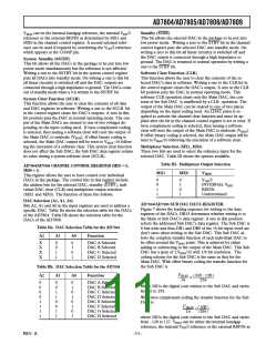
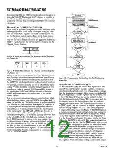
AD7804/AD7808 INTERFACE SECTION
sequence for the channel control register write, and Figures 6
and 7 show the sequence for loading data to the Main and Sub
DAC data registers. Figure 3 shows the internal registers associ-
ated with the AD7804/AD7808 serial interface DACs. Only one
DAC structure is shown for clarity.
The AD7804 and AD7808 are serial input devices. Three lines
control the serial interface, FSIN, CLKIN and SDIN. The timing
diagram is shown in Figure 1.
Two mode bits (MD1 and MD0) which are DB13 and DB14 of
the serial word written to the AD7804/AD7808 are used to deter-
mine whether writing is to the DAC data registers or the control
registers of the device. These parts contain a system control
register for controlling the operation of all DACs in the package
as well as a channel control register for controlling the operation of
each individual DAC. Table I shows how to access these registers.
FSIN
CLKIN
SDIN
16-BIT
INPUT SHIFT REGISTER
DECODER
SYSTEM
CONTROL
REGISTER
Table I. Register Selection Table for the AD7804/AD7808
CHANNEL
CONTROL
REGISTER
DATA REGISTER
DATA REGISTER
TO ALL
CHANNELS
MD1
MD0
Function
10
8
DAC REGISTER
DAC REGISTER
0
0
1
0
1
X
Write enable to system control register.
Write enable to channel control register.
Write enable to DAC data registers.
SINGLE
CHANNEL
10
8
8-BIT DAC
(SUB DAC)
10-BIT DAC
(MAIN DAC)
V
OUT
V
INTERNAL V
BIAS
REF
/2
When the FSIN input goes low, data appearing on the SDIN
line is clocked into the input register on each falling edge of
CLKIN. Data to be transferred to the AD7804/AD7808 is
loaded MSB first. Figure 4 shows the loading sequence for the
AD7804/AD7808 system control register, Figure 5 shows the
V
MUX
DD
REFIN
Figure 3. AD7804/AD7808 Internal Registers
REV. A
–9–

 ETC [ ETC ]