AD7804/AD7805/AD7808/AD7809
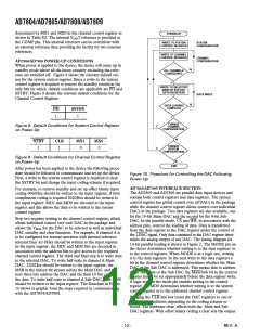
MSB
LSB
X
MD0 = 0 MD1 = 0
X
X
X
X
X
0
BIN/COMP
PD SSTBY SCLR
0
X
X
X = Don’t Care
Figure 4. AD7804/AD7808 System Control Register Loading Sequence
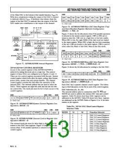
DB15 (MSB)
DB0 (LSB)
X
MD0 = 1 MD1 = 0 A2* A1
A0
MX1 MX0
X
X
X
STBY
CLR
0
X
X
X = Don’t Care
*Applicable to the AD7808 Only, and Are Don’t Care Conditions when Operating the AD7804.
Figure 5. AD7804/AD7808 Channel Control Register Loading Sequence
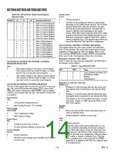
DB15 (MSB)
DB0 (LSB)
MAIN/SUB MD0 = X MD1 = 1 A2* A1 A0
DB9 DB8 DB7 DB6 DB5 DB4 DB3 DB2
DB1 DB0
X = Don’t Care
*Applicable to the AD7808 Only, and Are Don’t Care Conditions when Operating the AD7804.
Figure 6. AD7804/AD7808 Main DAC Data Register Loading Sequence (MAIN/SUB = 0)
DB15 (MSB)
DB0 (LSB)
MAIN/SUB MD0 = X MD1 = 1 A2* A1 A0
DB7 DB6 DB5 DB4 DB3 DB2 DB1 DB0
X
X
X = Don’t Care
*Applicable to the AD7808 Only, and Are Don’t Care Conditions when Operating the AD7804.
Figure 7. AD7804/AD7808 Sub DAC Data Register Loading Sequence (MAIN/SUB = 1)
AD7804/AD7808 SYSTEM CONTROL REGISTER (MD1 = 0,
MD0 = 0)
The bits in this register allow control over all DACs in the
package. The control bits include power down (PD), DAC input
coding select (BIN/COMP), system standby (SSTBY) and a
system clear (SCLR). The function of these bits is as follows:
When the system control register is selected by writing zeros to
the mode bits, MD1 and MD0 the address bits are ignored as
the system control register controls all DACs in the package.
When MD1 = 0 and MD0 = 1, writing is to the channel control
register. Only the DAC selected by the address bits will be af-
fected by writing to this register. Each individual DAC has a
channel control register.
Power Down (PD)
This bit in the control register is used to shut down the complete
device. With a 0 in this position, the reference and all DACs are
put into low power mode. Writing a 1 to this bit puts the part in
the normal operating mode. When in power-down mode, the
contents of all registers are retained and are valid when the
device is put back into normal operation.
The DACs data registers are addressed by writing a one to
MD1 (DB13); the condition of MD0 (DB14) does not matter
when writing to the data registers. DB15 determines whether
writing is to the Main DAC data register or to the Sub DAC
data register. The Main DAC is 10 bits wide and the Sub DAC
is 8 bits wide. Thus when writing to the Sub DAC DB1 and
DB0 become don’t cares. The Sub DAC is used to offset the
complete transfer function of the Main DAC around its VBIAS
point. The Sub DAC has 1/8 LSB resolution and will enable the
transfer function of the Main DAC to be offset by ± VBIAS/32.
Coding (BIN/COMP)
This bit in the system control register allows the user to select
one of two input coding schemes. The available schemes are
Twos complement coding and offset binary coding. All DACs
will be configured with the same input coding scheme. Writing
a zero to the control register selects twos complement coding,
while writing a 1 to this bit in the control register selects offset
binary coding.
When the LDAC line goes low, all DAC registers in the device
are simultaneously loaded with the contents of their respective
DAC data registers, and the outputs change accordingly.
Bringing the CLR line low resets the DAC data and DAC regis-
With twos complement coding selected the output voltage from
the Main DAC is of the form :
ters. This hardware clear affects both the Main and Sub DACs.
This operation sets the analog output of the Main DAC to VBIAS
16 when offset binary coding is selected and the output is set to
VBIAS when twos complement coding is used. VBIAS is the output
of the internal multiplexer as shown in Figure 3. The output of
the Sub DAC is used to shift the transfer function of the Main
DAC around the VBIAS point and the contribution from the Sub
DAC is zero following an external hardware clear. Software
clears affect the Main DACs only.
/
VOUT = VBIAS ± VSWING
where
15
16
VSWING is
×VBIAS
With Offset Binary coding selected the output voltage from the
Main DAC ranges from:
VBIAS
16
31
16
V
×
BIAS
VOUT
=
to VOUT
=
–10–
REV. A

 ETC [ ETC ]