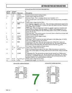
AD7804/AD7805/AD7808/AD7809
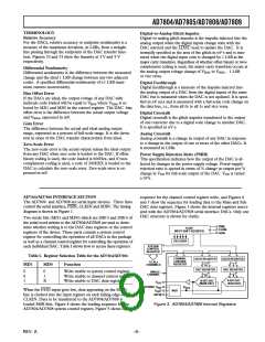
AD7805/AD7809 TIMING CHARACTERISTICS1
(VDD = 3.3 V ؎ 10% to 5 V ؎ 10%; AGND = DGND = 0 V; Reference
= Internal Reference. All specifications TMIN to TMAX unless otherwise noted.)
Limit at TMIN, TMAX
All Versions
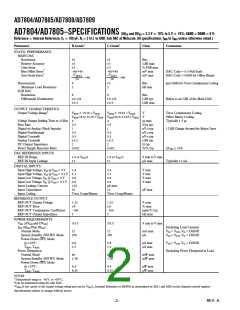
Parameter
Unit
Description
t1
t2
t3
t4
t5
t6
t6A
t7
t8
25
4.5
25
4.5
25
4.5
6
40
0
40
100
40
100
ns min
ns min
ns min
ns min
ns min
ns min
ns min
ns min
ns min
ns min
ns min
ns min
ns min
Mode Valid to Write Setup Time
Mode Valid to Write Hold Time
Address Valid to Write Setup Time
Address Valid to Write Hold Time
Data Setup Time
Data Hold Time
LDAC Valid to Write Hold Time
Chip Select to Write Setup Time
Chip Select to Write Hold Time
Write Pulsewidth
Time Between Successive Writes
LDAC, CLR Pulsewidth
t9
t10
t11
t12
Write to LDAC Setup Time
NOTE
1Sample tested during initial release and after any redesign or process change that may affect this parameter. All input signals are specified with tr = tf = 5 ns and
timed from a voltage of (VIL + VIH)/2.
Specifications subject to change without notice.
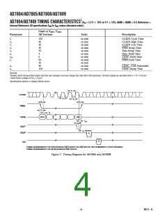
t1
t2
MODE
t4
t3
A0, A1, A2
t8
t7
CS
t10
t9
WR
t6
t5
DATA
t6A
1
LDAC
t11
t12
2
LDAC
t11
CLR
1
2
TIMING REQUIREMENTS FOR SYNCHRONOUS LDAC UPDATE OR LDAC MAY BE TIED PERMANENTLY LOW IF REQUIRED.
TIMING REQUIREMENTS FOR ASYNCHRONOUS LDAC UPDATE.
Figure 2. Timing Diagram for AD7805/AD7809 Parallel Write
REV. A
–5–

 ETC [ ETC ]