AD7804/AD7805/AD7808/AD7809
VBIAS can be the internal bandgap reference, the internal VDD/2
reference or the external REFIN as determined by MX1 and
MX0 in the channel control register. A second external refer-
ence can be used if required by overdriving the VDD/2 reference
which appears at the COMP pin.
Standby (STBY)
This bit allows the selected DAC in the package to be put into
low power mode. Writing a zero to the STBY bit in the channel
control register puts the selected DAC into standby mode. On
writing a zero to this bit all linear circuitry is switched off and
the DAC output is connected through a high impedance to
ground. The DAC is returned to normal operation by writing a
one to the STBY bit.
System Standby (SSTBY)
This bit allows all the DACs in the package to be put into low
power mode simultaneously but the reference is not affected.
Writing a one to the SSTBY bit in the system control register
puts all DACs into standby mode. On writing a one to this bit
all linear circuitry is switched off and the DAC outputs are
connected through a high impedance to ground. The DACs come
out of standby mode when a 0 is written to the SSTBY bit.
Software Clear Function (CLR)
This function allows the user to clear the contents of the se-
lected DAC’s data in software. Writing a one to the CLR bit in
the control register clears the DAC’s output. A zero in the CLR
bit position puts the DAC in normal operating mode. This
software CLR operation clears only the Main DAC, the con-
tents of the Sub DAC is unaffected by a CLR operation. The
output of the Main DAC can be cleared to one of two places
depending on the input coding used. An LDAC pulse is re-
quired to activate the channel clear function and must be ap-
plied after the bit in the channel control register is set or reset. If
twos complement coding is selected, then issuing a software
clear will reset the output of the Main DAC to midscale (VBIAS).
If offset binary coding is selected, the Main DAC output will be
reset to VBIAS/16 following the execution of a software clear.
System Clear Function (SCLR)
This function allows the user to clear the contents of all data
and DAC registers in software. Writing a one to the SCLR bit
in the control register clears the DAC’s outputs. A zero in this
bit position puts the DAC in normal operating mode. The out-
put of the Main DACs are cleared to one of two voltages de-
pending on the input coding used. If twos complement coding
is selected, then issuing a software clear will reset the output of
the Main DAC to midscale (VBIAS). If offset binary coding is
selected, the Main DAC output will be reset to VBIAS /16 follow-
ing the execution of a software clear. This system clear function
does not affect the Sub DAC; the Sub DAC data register retains
its value during a system software clear (SCLR).
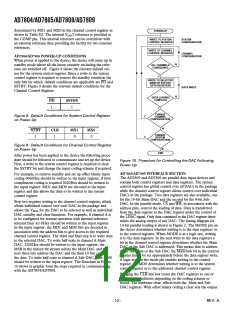
Multiplexer Selection (MX1, MX0)
These two bits are used to select the reference input for the
selected DAC. Table III shows the options available.
Table III. Multiplexer Output Selection
AD7804/AD7808 CHANNEL CONTROL REGISTER (MD1 = 0,
MD0 = 1)
MX1
MX0
VBIAS
This register allows the user to have control over individual
DACs in the package. The control bits in this register include
the address bits for the selected DAC, standby (STBY), indi-
vidual DAC clear (CLR) and multiplexer output selection
(MX1 and MX0). The function of these bits follows.
0
0
1
1
0
1
0
1
VDD/2
INTERNAL VREF
REFIN
Undetermined
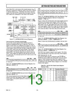
DAC Selection (A2, A1, A0)
AD7804/AD7808 SUB DAC DATA REGISTER
Bits A2, A1 and A0 in the input registers are used to address a
specific DAC. Table IIa shows the selection table for the DACs
of the AD7804. Table IIb shows the selection table for the
DACs of the AD7808.
Figure 7 shows the loading sequence for writing to the data
registers of the DACs. DB15 determines whether writing is to
the Main or Sub DAC’s data register. A one in this position
selects the addressed Sub DAC’s data register. The Sub DAC is
8 bits wide and thus DB1 and DB0 of the 16-bit input word are
don’t cares when writing to the Sub DAC. This Sub DAC al-
lows the complete transfer function of each individual DAC to
be offset around the VBIAS point. This is achieved by either
adding or subtracting to the output of the Main DAC. This Sub
DAC has a span of ±VBIAS/32 with 1/8-bit resolution. The
coding scheme for the Sub DAC is the same as that for the
Main DAC. With offset binary coding the transfer function for
the Sub DAC is
Table IIa. DAC Selection Table for the AD7804
A2
A1
A0
Function
X
X
X
X
0
0
1
1
0
1
0
1
DAC A Selected
DAC B Selected
DAC C Selected
DAC D Selected
Table IIb. DAC Selection Table for the AD7808
VBIAS
16
A2
A1
A0
Function
(NB –128)
×
256
0
0
0
0
1
1
1
1
0
0
1
1
0
0
1
1
0
1
0
1
0
1
0
1
DAC A Selected
DAC B Selected
DAC C Selected
DAC D Selected
DAC E Selected
DAC F Selected
DAC G Selected
DAC H Selected
where NB is the digital code written to the Sub DAC and varies
from 0 to 255.
With twos complement coding the transfer function for the Sub
DAC is
VBIAS
16
NB
×
(
)
256
where NB is the digital code written to the Sub DAC and varies
from –128 to 127. VBIAS can be either the internal bandgap
reference, the internal VDD/2 reference or the external REFIN as
REV. A
–11–

 ETC [ ETC ]