PIC12F510/16F506
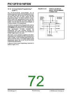
FIGURE 10-16:
TYPICAL IN-CIRCUIT
SERIAL PROGRAMMING
CONNECTION
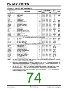
10.12 In-Circuit Serial Programming™
(ICSP™)
The PIC12F510/16F506 microcontrollers can be
serially programmed while in the end application circuit.
This is simply done with two lines for clock and data,
and three other lines for power, ground and the
programming voltage. This allows customers to manu-
facture boards with unprogrammed devices and then
program the microcontroller just before shipping the
product. This also allows the most recent firmware, or
a custom firmware, to be programmed.
To Normal
Connections
PIC12F510
PIC16F506
External
Connector
Signals
+5V
0V
VDD
VSS
VPP
MCLR/VPP
The devices are placed into a Program/Verify mode by
holding the GP1/RB1 and GP0/RB0 pins low while rais-
ing the MCLR (VPP) pin from VIL to VIHH (see program-
GP1/RB1
GP0/RB0
CLK
Data I/O
ming
specification).
GP1/RB1
becomes
the
programming clock and GP0/RB0 becomes the
programming data. Both GP1/RB1 and GP0/RB0 are
Schmitt Trigger inputs in this mode.
VDD
To Normal
Connections
After Reset, a 6-bit command is supplied to the device.
Depending on the command and if the command was a
Load or a Read, 14 bits of program data are then sup-
plied to or from the device. For complete details of serial
programming, please refer to the PIC12F510/16F506
Programming Specifications.
A typical In-Circuit Serial Programming connection is
shown in Figure 10-16.
DS41268B-page 70
Preliminary
© 2006 Microchip Technology Inc.

 ETC [ ETC ]