PIC12F510/16F506
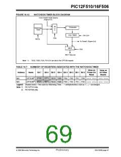
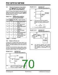
FIGURE 10-14:
BROWN-OUT
PROTECTION CIRCUIT 2
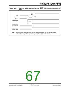
10.7 Time-out Sequence, Power-down
and Wake-up from Sleep Status
Bits (TO, PD, GPWUF/RBWUF)
VDD
VDD
The TO, PD and (GPWUF/RBWUF) bits in the STATUS
register can be tested to determine if a Reset condition
has been caused by a power-up condition, a MCLR or
Watchdog Timer (WDT) Reset.
R1
R2
PIC12F510
PIC16F506
Q1
(2)
MCLR
(1)
40k
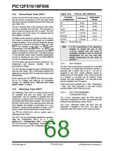
TABLE 10-8: TO/PD/(GPWUF/RBWUF)
STATUS AFTER RESET
GPWUF/
RBWUF
CWUF
TO PD
Reset Caused By
Note 1: This brown-out circuit is less expensive,
although less accurate. Transistor Q1 turns
off when VDD is below a certain level such
that:
0
0
0
0
1
0
u
0
WDT wake-up from
Sleep
0
0
0
0
WDT time-out (not
from Sleep)
R1
= 0.7V
VDD •
R1 + R2
MCLR wake-up from
Sleep
2: Pin must be configured as MCLR.
0
0
0
0
1
u
1
u
Power-up
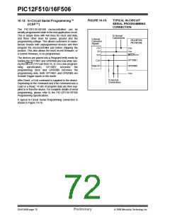
FIGURE 10-15:
BROWN-OUT
PROTECTION CIRCUIT 3
MCLR not during
Sleep
VDD
0
1
1
0
1
1
0
0
Wake-up from Sleep
on pin change
MCP809
VDD
Bypass
Capacitor
Wake-up from Sleep
on comparator
change
VSS
VDD
RST
MCLR
Legend: u= unchanged
PIC12F510
PIC16F506
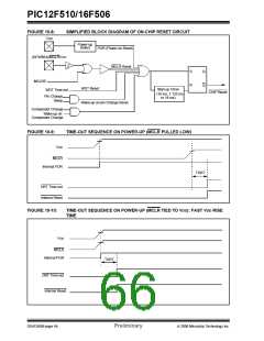
10.8 Reset on Brown-out
A brown-out is a condition where device power (VDD)
dips below its minimum value, but not to zero, and then
recovers. The device should be reset in the event of a
brown-out.
Note:
This brown-out protection circuit employs
Microchip Technology’s MCP809 microcon-
troller supervisor. There are 7 different trip
point selections to accommodate 5V to 3V
systems.
To reset PIC12F510/16F506 devices when a brown-
out occurs, external brown-out protection circuits may
be built, as shown in Figure 10-13 and Figure 10-14.
FIGURE 10-13:
BROWN-OUT
PROTECTION CIRCUIT 1
VDD
VDD
33k
PIC12F510
PIC16F506
Q1
(2)
MCLR
10k
(1)
40k
Note 1: This circuit will activate Reset when VDD goes
below Vz + 0.7V (where Vz = Zener voltage).
2: Pin must be configured as MCLR.
DS41268B-page 68
Preliminary
© 2006 Microchip Technology Inc.

 ETC [ ETC ]