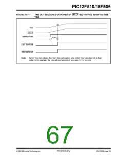
PIC12F510/16F506
10.9 Power-Down Mode (Sleep)
Note 1: Caution: Right before entering Sleep,
read the comparator Configuration
register(s) CM1CON0 and CM2CON0.
When in Sleep, wake-up occurs when the
comparator output bit C1OUT and
C2OUT change from the state they were
in at the last reading. If a wake-up on
comparator change occurs and the pins
are not read before re-entering Sleep, a
wake-up will occur immediately, even if
no pins change while in Sleep mode.
A device may be powered down (Sleep) and later
powered up (wake-up from Sleep Reset).
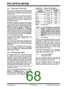
10.9.1
SLEEP
The Power-Down mode is entered by executing a
SLEEPinstruction.
If enabled, the Watchdog Timer will be cleared but
keeps running, the TO bit (STATUS<4>) is set, the PD
bit (STATUS<3>) is cleared and the oscillator driver is
turned off. The I/O ports maintain the status they had
before the SLEEP instruction was executed (driving
high, driving low or high-impedance).
2: For 16F506 only.
The WDT is cleared when the device wakes from
Sleep, regardless of the wake-up source.
Note:
A device Reset generated by a WDT
time-will not drive the MCLR pin low.
For lowest current consumption while powered down,
all input pins should be at VDD or VSS and (GP3/RB3)/
MCLR/VPP pin must be at a logic high level if MCLR is
enabled.
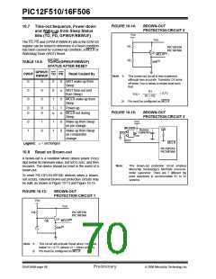
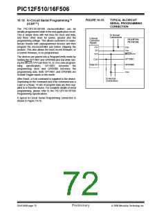
10.10 Program Verification/Code
Protection
If the code protection bit has not been programmed, the
on-chip program memory can be read out for
verification purposes.
10.9.2
WAKE-UP FROM SLEEP RESET
The device can wake-up from Sleep through one of the
following events:
The first 64 locations and the last location (OSCCAL)
can be read, regardless of the code protection bit
setting.
1. An external Reset input on (GP3/RB3)/MCLR/
VPP pin when configured as MCLR.
The last memory location can be read regardless of the
code protection bit setting on the PIC12F510/16F506
devices.
2. A Watchdog Timer Time-out Reset (if WDT was
enabled).
3. A change-on-input pin GP0/RB0, GP1/RB1,
GP3/RB3 or RB4 when wake-up on change is
enabled.
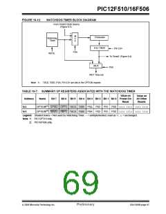
10.11 ID Locations
Four memory locations are designated as ID locations
where the user can store checksum or other code
identification numbers. These locations are not
accessible during normal execution, but are readable
and writable during Program/Verify.
4. A change in the comparator ouput bits, C1OUT
and C2OUT (if comparator wake-up is enabled).
These events cause a device Reset. The TO, PD,
CWUF and GPWUF/RBWUF bits can be used to deter-
mine the cause of device Reset. The TO bit is cleared
if a WDT time-out occurred (and caused wake-up). The
PD bit, which is set on power-up, is cleared when
SLEEPis invoked. The CWUF bit indicates a change in
comparator output state while the device was in Sleep.
The GPWUF/RBWUF bit indicates a change in state
while in Sleep at pins GP0/RB0, GP1/RB1, GP3/RB3
or RB4 (since the last file or bit operation on GP/RB
port).
Use only the lower 4 bits of the ID locations and always
set the upper 4 bits as ‘1’s. The upper 4 bits are
unimplemented.
These locations can be read regardless of the code
protect setting.
Note:
Caution: Right before entering Sleep,
read the input pins. When in Sleep, wake-
up occurs when the values at the pins
change from the state they were in at the
last reading. If a wake-up on change
occurs and the pins are not read before
reentering Sleep, a wake-up will occur
immediately even if no pins change while
in Sleep mode.
© 2006 Microchip Technology Inc.
Preliminary
DS41268B-page 69

 ETC [ ETC ]