PIC12F510/16F506
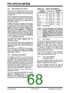
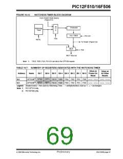
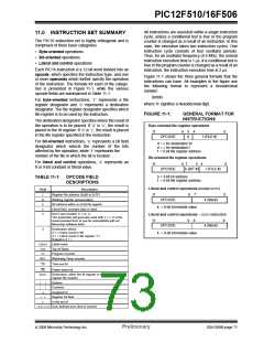
FIGURE 10-12:
WATCHDOG TIMER BLOCK DIAGRAM
From Timer0 Clock Source
(Figure 6-5)
0
M
U
X
Postscaler
1
Watchdog
Timer
8-to-1 MUX
PS<2:0>
PSA
WDTE
(Figure 6-4)
To Timer0
0
1
MUX
PSA
WDT Time-out
Note 1: T0CS, T0SE, PSA, PS<2:0> are bits in the OPTION register.
TABLE 10-7: SUMMARY OF REGISTERS ASSOCIATED WITH THE WATCHDOG TIMER
Value on
Value on
All Other
Resets
Address
Name
Bit 7
Bit 6
Bit 5 Bit 4 Bit 3 Bit 2 Bit 1 Bit 0 Power-On
Reset
N/A
N/A
OPTION(1) GPWU GPPU T0CS T0SE PSA PS2 PS1 PS0 1111 1111 1111 1111
OPTION(2) RBWU RBPU T0CS T0SE PSA PS2 PS1 PS0 1111 1111 1111 1111
Legend: Shaded boxes = Not used by Watchdog Timer. – = unimplemented, read as ‘0’, u= unchanged.
Note 1: PIC12F510 only.
2: PIC16F506 only.
© 2006 Microchip Technology Inc.
Preliminary
DS41268B-page 67

 ETC [ ETC ]