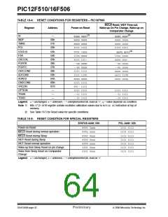
PIC12F510/16F506
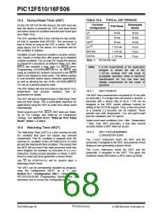
TABLE 10-6: TYPICAL DRT PERIODS
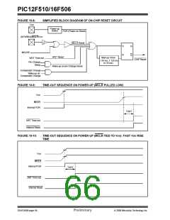
10.5 Device Reset Timer (DRT)
Oscillator
Configuration
Subsequent
On the PIC12F510/16F506 devices, the DRT runs any
time the device is powered up. DRT runs from Reset
and varies based on oscillator selection and Reset type
(see Table 10-6).
POR Reset
Resets
LP
18 ms
18 ms
18 ms
18 ms
18 ms
10 μs
10 μs
10 μs
XT
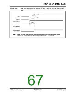
The DRT operates from a free running on-chip oscilla-
tor that is separate from INTOSC. The processor is
kept in Reset as long as the DRT is active. The DRT
delay allows VDD to rise above VDD minimum and for
the oscillator to stabilize.
HS(1)
18 ms
EC(1)
1.125 ms
1.125 ms
1.125 ms
INTOSC
EXTRC
Oscillator circuits, based on crystals or ceramic resona-
tors, require a certain time after power-up to establish
a stable oscillation. The on-chip DRT keeps the devices
in a Reset for a set period, as stated in Table 10-6, after
MCLR has reached a logic high (VIH MCLR) level.
Programming (GP3/RB3)/MCLR/VPP as MCLR and
using an external RC network connected to the MCLR
input is not required in most cases. This allows savings
in cost-sensitive and/or space restricted applications,
as well as allowing the use of the (GP3/RB3)/MCLR/
VPP pin as a general purpose input.
Note 1: PIC16F506 only
Note:
It is the responsibility of the application
designer to ensure the use of the
1.125 ms nominal DRT will result in
acceptable operation. Refer to Electrical
Specifications for VDD rise time and
stability requirements for this mode of
operation.
The DRT delays will vary from chip-to-chip due to VDD,
temperature and process variation. See AC
parameters for details.
10.6.1
WDT PERIOD
The WDT has a nominal time-out period of 18 ms (with
no prescaler). If a longer time-out period is desired, a
prescaler with a divisor ratio of up to 1:128 can be
assigned to the WDT (under software control) by
writing to the OPTION register. Thus, a time-out period
of a nominal 2.3 seconds can be realized. These
periods vary with temperature, VDD and part-to-part
process variations (see DC specs).
The DRT will also be triggered upon a Watchdog Timer
time-out from Sleep. This is particularly important for
applications using the WDT to wake from Sleep mode
automatically.
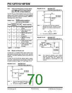
Reset sources are POR, MCLR, WDT time-out, Wake-
up on Pin Change and Wake-up on Comparator
Change. See Section 10.9.2 “Wake-up from Sleep
Reset”, Notes 1, 2 and 3.
Under worst case conditions (VDD = Min., Temperature
= Max., max. WDT prescaler), it may take several
seconds before a WDT time-out occurs.
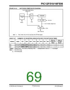
10.6 Watchdog Timer (WDT)
10.6.2
WDT PROGRAMMING
CONSIDERATIONS
The Watchdog Timer (WDT) is a free running on-chip
RC oscillator that does not require any external
components. This RC oscillator is separate from the
external RC oscillator of the (GP5/RB5)/OSC1/CLKIN
pin and the internal 4/8 MHz oscillator. This means that
the WDT will run even if the main processor clock has
been stopped, for example, by execution of a SLEEP
instruction. During normal operation or Sleep, a WDT
Reset or wake-up Reset generates a device Reset.
The CLRWDT instruction clears the WDT and the
postscaler, if assigned to the WDT, and prevents it from
timing out and generating a device Reset.
The SLEEP instruction resets the WDT and the
postscaler, if assigned to the WDT. This gives the
maximum Sleep time before a WDT wake-up Reset.
The TO bit (STATUS<4>) will be cleared upon a
Watchdog Timer Reset.
The WDT can be permanently disabled by program-
ming the configuration WDTE as
a
‘0’ (see
Section 10.1 “Configuration Bits”). Refer to the
PIC12F510/16F506 Programming Specifications to
determine how to access the Configuration Word.
DS41268B-page 66
Preliminary
© 2006 Microchip Technology Inc.

 ETC [ ETC ]