Freescale Semiconductor, Inc.
Software Design
Algorithm of Dead Time Distortion Correction
Algorithm
enabled
INITIAL
STATE
0
1
Initial recognition of
00
positive current
00
00
2
00
High positive
current
Low negative
current
X1/1
3
X0/0
4
Waits for high
Change IPOL
(current treshold
crossing)
Waits for high
positive current
negative current
|θ−θC|>80o / 0
|θ−θC|>80o/1
6
High negative
current
5
0X/0
Low positive
current
1X/1
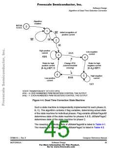
STATE TRANSITION KEY: DT1 DT2 / IPOL
ODD-NUMBERED PWM REGISTERS CONTROL THE OUTPUT
IPOL = 0: ODD NUMBERED PWM REGISTER CONTROLS OUTPUT
EVEN-NUMBERED PWM REGISTERS CONTROL THE OUTPUT
IPOL = 1: EVEN NUMBERED PWM REGISTER CONTROLS OUTPUT
Figure 4-4. Dead Time Correction State Machine
Such a state machine is independently implemented for each phase (A,
B, C). The algorithm contains 2 flag variables, determining actual state
of the state machine for individual phases. Flag variable dtStateFlagsAB
determines state of the state machine for phases A & B, dtStateFlagsC
determines state of the state machine for phase C.
The meaning of individual bits of dtStateFlagsAB is listed in Table 4-1.
The meaning of individual bits of dtStateFlagsC is listed in Table 4-2.
DRM019 — Rev 0
MOTOROLA
Designer Reference Manual
45
Software Design
For More Information On This Product,
Go to: www.freescale.com

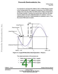
 ETC [ ETC ]