Freescale Semiconductor, Inc.
Software Design
Data Flow
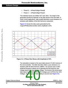
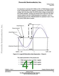
It is important to note that 50% PWM (or 50% of PWM Modulus loaded
to the corresponding PVAL registers) corresponds to the ZERO phase
voltage. But in the wave table, the ZERO phase voltage corresponds to
the number #0x0000. Therefore the fetched wave value from the table
must be added to the 50% PWM Modulation for quadrant 1 and 2 or
substracted from the 50% PWM Modulation for quadrant 3 and 4. Thus
the correct PWM value is loaded.
0x7fff
0x7fff
ActualPhase(n)
Actual Phase (n)
PhaseIncrement
Phase Increment
ActualPhase(n-1)
Actual Phase (n–1)
0x4000
0x4000
(DutyCycle.PhaseA)
(DutyCycle.PhaseA)
0x0000
0x0000
o
0x8000 = –180°
0x8000 = -180
0
0x7fff = 180°o
0
0x7fff = 180
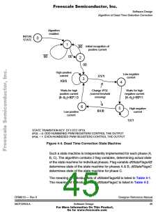
Figure 4-3. mcgen3PhWaveSine Data Explanation - Phase A
The output parameters of the process are:
• PWM value for phase A: PVAL1 register
• PWM value for phase B: PVAL3 register
• PWM value for phase C: PVAL5 register
DRM019 — Rev 0
MOTOROLA
Designer Reference Manual
41
Software Design
For More Information On This Product,
Go to: www.freescale.com

 ETC [ ETC ]