Freescale Semiconductor, Inc.
System Description
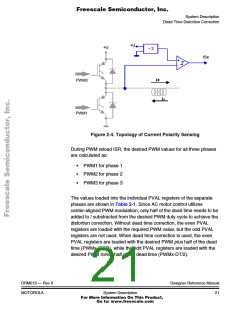
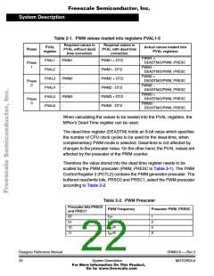
Table 2-1. PWM values loaded into registers PVAL1-6
Required values in
PVAL without dead
time correction
Required values in
PVAL with dead time
correction
PVAL
register
Actual values loaded into
PVAL registers
Phase
PWM1 +
DEADTM/2/PWM_PRESC
PVAL1
PVAL2
PVAL3
PVAL4
PVAL5
PVAL6
PWM1
PWM1 + DT/2
PWM1 - DT/2
PWM2 + DT/2
PWM2 - DT/2
PWM3 + DT/2
PWM3 - DT/2
Phase
1
PWM1 -
DEADTM/2/PWM_PRESC
PWM2 +
DEADTM/2/PWM_PRESC
PWM2 -
DEADTM/2/PWM_PRESC
-
PWM2
Phase
2
-
PWM3 +
DEADTM/2/PWM_PRESC
PWM3 -
DEADTM/2/PWM_PRESC
PWM3
-
Phase
3
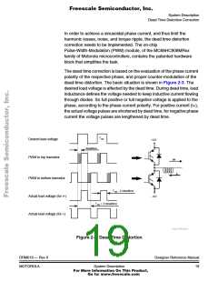
When calculating the values to be loaded into the PVAL registers, the
MRxx’s Dead Time register can be used.
The dead-time register (DEADTM) holds an 8-bit value which specifies
the number of CPU clock cycles to be used for the dead-time, when
complementary PWM mode is selected. Dead-time is not affected by
changes to the prescaler value. On the other hand, the PVAL values are
affected by the prescaler of the PWM counter.
Therefore the value stored into the dead time register needs to be
scalled by the PWM prescaler (PWM_PRESC in Table 2-1). The PWM
Control Register 2 (PCTL2) contains the PWM generator prescaler. The
buffered read/write bits, PRSC0 and PRSC1, select the PWM prescaler
according to Table 2-2.
Table 2-2. PWM Prescaler
Prescaler bits PRSC0
and PRSC1
PWM Frequency
Prescaler PWM_PRESC
f
00
01
10
11
1
2
4
8
OP
f
f
f
/2
/4
/8
OP
OP
OP
Designer Reference Manual
22
DRM019 — Rev 0
MOTOROLA
System Description
For More Information On This Product,
Go to: www.freescale.com

 ETC [ ETC ]